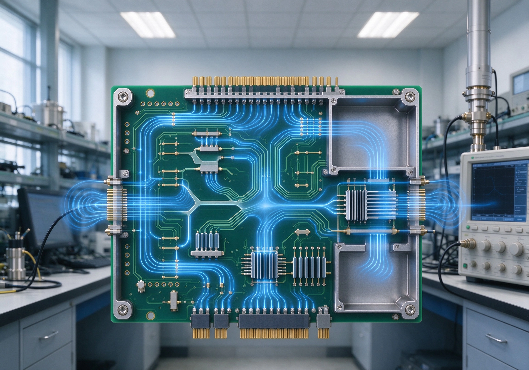
Radio frequency (RF) systems power critical modern technologies from 5G communications and radar systems to Satellite Communications, autonomous vehicle sensors, and Medical Imaging equipment. These systems operate at frequencies ranging from 1GHz to well over 100GHz for millimeter-wave applications, and their performance is highly dependent on the quality of the underlying printed circuit board. Unlike standard low-frequency PCBs, high-frequency RF PCBs require specialized design practices, carefully selected materials, and Precision Manufacturing processes to deliver consistent, reliable performance. Even minor design imperfections or manufacturing variations can cause significant Signal Loss, reduced range, increased noise, or complete system failure in RF applications. Custom high frequency PCB design and fabrication tailored to your specific RF system requirements is essential for achieving optimal performance and reliability.

Unique Requirements of High Frequency RF PCBs
High frequency signals behave very differently from low-frequency digital or analog signals, creating unique requirements for PCB design and manufacturing:
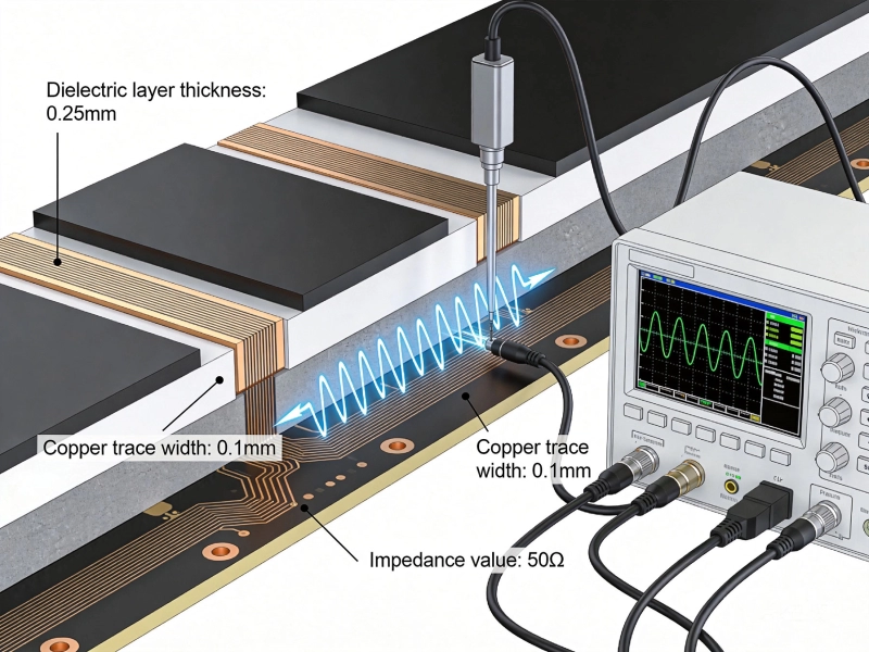
- Precise Impedance Control: Most RF systems require 50 ohm (or sometimes 75 ohm) Controlled Impedance across all RF signal paths. Even small impedance variations of 5-10 ohms can cause significant Signal Reflection and loss.
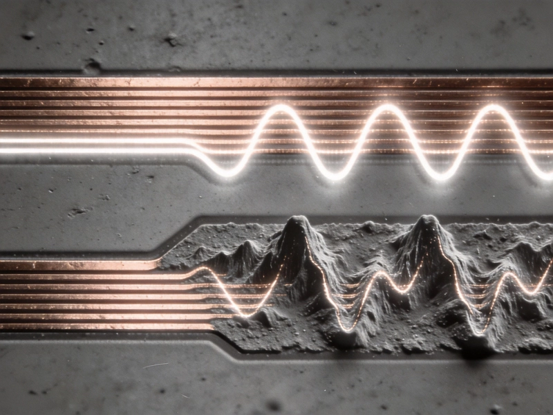
- Low Signal Loss: High frequency signals suffer from increased attenuation as they travel through Pcb Materials and traces. Minimizing Insertion Loss is critical for maintaining signal strength and system sensitivity.
- Minimal signal radiation: RF signals can easily radiate from unshielded traces, causing Electromagnetic Interference (Emi) with other circuits and reducing overall system efficiency.
- Immunity to external interference: RF systems, especially receivers, are highly sensitive to external noise and interference. Proper Shielding and isolation are required to prevent unwanted signals from degrading performance.
- Consistent material properties: The electrical properties of Pcb Materials (Dielectric Constant, Dissipation Factor) must remain consistent across the entire board and over temperature and frequency variations to ensure predictable RF performance.
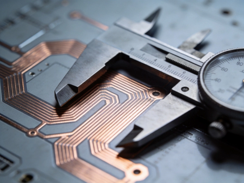
- Tight manufacturing tolerances: High frequency designs require much tighter manufacturing tolerances for trace width, spacing, dielectric thickness, and via placement than standard PCBs, as even minor variations can significantly impact RF performance.
Meeting these requirements requires a specialized approach to both design and manufacturing that goes far beyond standard PCB practices.
Key Design Considerations for Custom High Frequency RF PCBs
Successful high frequency PCB design starts with careful planning and attention to detail at every stage of the design process:
1. Material Selection
Material selection is the single most important factor in high frequency pcb performance. The right material depends on your operating frequency, performance requirements, thermal constraints, and budget:
- Fr-4: Standard Fr-4 can be used for lower RF frequencies up to 2-3 GHz, but its higher Dissipation Factor (Df) and inconsistent Dielectric Constant (Dk) make it unsuitable for higher frequencies. High-performance FR-4 variants with controlled Dk/Df are available for mid-range RF applications up to 5-6 GHz.
- Ptfe-based materials: Polytetrafluoroethylene (Ptfe) composite materials (such as Rogers, Taconic, or Arlon materials) are the most common choice for high frequency applications above 3 GHz. These materials offer low Dk (typically 2.2-10.2 depending on formulation), very low Df (0.001-0.005), and stable electrical properties over wide frequency and temperature ranges.
- Ceramic-filled PTFE materials: For millimeter-wave applications above 30 GHz, ceramic-filled PTFE materials provide the highest performance, with extremely stable Dk values and very low loss at high frequencies.
- Hybrid material stacks: For mixed-signal designs with both RF and digital circuitry, hybrid stacks combining high-frequency PTFE materials for RF layers and standard FR-4 for digital layers offer a cost-effective solution that meets both performance and budget requirements.
Always select materials with specified Dk tolerance (preferably ±5% or better) and guaranteed Df values for your operating frequency range. Avoid generic materials with unspecified electrical properties.
2. Stackup Design
Careful stackup design is critical for achieving Controlled Impedance, minimizing loss, and providing proper Shielding:
- Impedance planning: Calculate required trace widths and dielectric thicknesses to achieve your target impedance (typically 50 ohms for single-ended RF signals, 100 ohms for differential pairs) for your selected material. Use a 2D or 3D field solver to verify impedance calculations, especially for complex Transmission Line structures.
- Transmission Line type: Choose the appropriate transmission line structure for your application: Microstrip (signal trace on outer layer over Ground Plane), stripline (signal trace between two ground planes), or coplanar waveguide (signal trace with ground planes on the same layer) for the best balance of performance and manufacturability.
- Ground Plane placement: Place a solid ground plane directly adjacent to all RF signal layers to provide a low-impedance return path, minimize radiation, and improve isolation between signal paths.
- Layer isolation: Separate RF signal layers from digital or noisy power layers with additional ground planes to prevent cross-interference.
3. Routing and Layout Best Practices
Follow these routing and layout guidelines to minimize signal loss and interference:
- Minimize RF trace lengths: Keep high-frequency signal paths as short and direct as possible to reduce Insertion Loss and radiation. Avoid unnecessary bends or stubs in RF traces.
- Avoid vias in RF paths: Vias introduce impedance discontinuities and signal loss. If you must transition a high-frequency signal between layers, use via fencing and ground vias adjacent to the signal via to minimize impedance mismatch and radiation.
- Maintain constant impedance: Keep trace widths consistent along all RF signal paths, and avoid transitions that change impedance. When bends are necessary, use curved or 45-degree bends instead of 90-degree corners to minimize impedance discontinuities.
- Provide adequate isolation: Separate high-power RF transmit paths from sensitive receive paths with sufficient spacing and shielding to prevent coupling and desensitization of the receiver. Use grounded guard traces between RF traces for additional isolation.
- Proper Grounding: Use large, continuous ground planes with no splits or gaps under RF signal paths. Place multiple ground vias around RF components and along Transmission Lines to provide a low-impedance return path and reduce radiation.
- Power supply filtering: Implement extensive power supply filtering for RF components, including multiple bypass capacitors of different values placed as close to component power pins as possible, to prevent noise from coupling into Rf Circuits through the power supply.
- Component Placement: Place RF components as close together as possible to minimize trace lengths between them. Match component footprints precisely to datasheet recommendations to avoid impedance mismatches at component interfaces.
4. Simulation and Validation
Use Electromagnetic Simulation tools throughout the design process to validate RF performance before manufacturing:
- Simulate impedance along all RF paths to ensure consistent performance.
- Run crosstalk and coupling analysis to verify isolation between sensitive signal paths.
- Perform S-parameter simulation to predict insertion loss, return loss, and isolation across your operating frequency range.
- Use 3D Electromagnetic Simulation for critical components such as antennas, filters, and high-frequency transitions to validate performance.
Critical Manufacturing Requirements for High Frequency PCBs
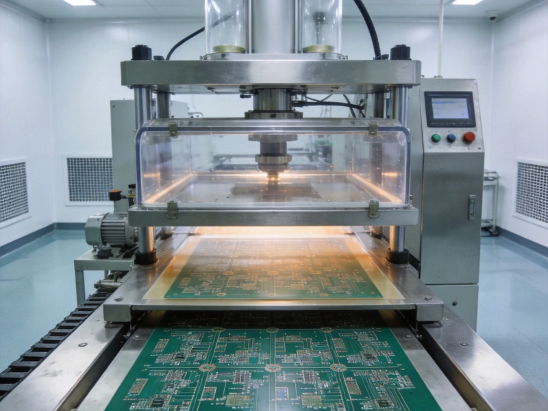
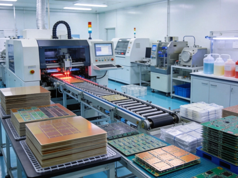
Even the best Rf Design will fail if not manufactured with proper processes and controls. When selecting a manufacturer for custom high frequency PCBs, ensure they have the capabilities and experience to meet these requirements:
- Tight tolerance control: Look for manufacturers that can hold trace width and spacing tolerances of ±10% or better, and dielectric thickness tolerances of ±5% or better, which are required for consistent Impedance Control.
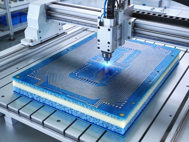
- Specialized material processing: High-frequency PTFE-based materials are softer and more difficult to process than standard FR-4. Ensure your manufacturer has experience processing your selected material, with proper process controls to avoid material deformation, delamination, or dimensional instability during manufacturing.
- Controlled impedance testing: Require 100% impedance testing of critical RF paths using time domain reflectometry (Tdr) to verify that impedance meets your specifications.
- Surface finish selection: Choose a surface finish suitable for high frequency applications. Electroless nickel immersion gold (ENIG) or immersion silver are the best choices for RF applications, as they provide a flat, consistent surface with low contact resistance. Avoid hot air solder leveling (HASL), which creates uneven surfaces that can cause impedance variations at high frequencies.
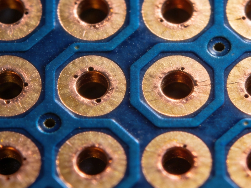
- Via processing: Ensure vias are properly plated and cleaned to avoid impedance variations and signal loss. For high-frequency applications, consider via filling or plating to improve electrical performance.
- Material traceability: Require full material traceability to ensure the actual materials used match your specified materials, with no substitutions that could impact RF performance.
- RF performance testing: For high-volume or high-reliability applications, work with manufacturers that can provide RF performance testing using network analyzers to validate insertion loss, return loss, and other key parameters across your operating frequency range.
Always work with your Pcb Manufacturer early in the design process to conduct a design for manufacturing (Dfm) review specific to high-frequency requirements. They can identify potential manufacturing issues that could impact RF performance and suggest design adjustments to improve manufacturability and reduce cost without sacrificing performance.
Common Applications for Custom High Frequency PCBs
Custom high frequency PCBs are used in a wide range of RF systems, including:
- 5G and 6G communications equipment: Base stations, user equipment, and antenna systems operating at sub-6GHz and millimeter-wave frequencies.
- Radar systems: Automotive Radar for autonomous vehicles, weather radar, air traffic control radar, and military radar systems operating from 24GHz to 77GHz and above.
- Satellite Communications: Satellite transceivers, ground station equipment, and user terminals operating at Ku-band, Ka-band, and higher frequencies.
- Medical devices: Medical Imaging equipment, patient monitoring systems, and RF-based therapeutic devices.
- Industrial and IoT systems: Industrial sensors, wireless communication modules, and IoT devices operating at sub-GHz, 2.4GHz, 5GHz, and mmWave frequencies.
- Aerospace and Defense Systems: Military communications equipment, electronic warfare systems, and navigation systems requiring high reliability and performance in extreme environments.
Conclusion
Designing and manufacturing custom high frequency PCBs for RF systems requires specialized knowledge, careful material selection, precision design practices, and strict manufacturing controls. By following proven design best practices, selecting appropriate materials, and working with an experienced Pcb Manufacturer that understands high-frequency requirements, you can achieve the consistent, reliable RF performance your system requires. Investing the time and resources to get your High-frequency Pcb design and fabrication right the first time will save you significant time and cost in testing, debugging, and redesign later, and ensure your RF system delivers the performance and reliability you expect.
Contact us to discuss your requirements.
Frequently Asked Questions
Q: What frequency range requires special high-frequency PCB design?
A: Special high-frequency design practices are generally recommended for signals above 1GHz, and are mandatory for signals above 3GHz or for high-performance applications at any frequency.
Q: How much more expensive are high-frequency PCBs compared to standard PCBs?
A: High-frequency PCBs using PTFE-based materials typically cost 2-5 times more than standard FR4 PCBs, depending on the material selected, design complexity, and order volume. Hybrid stackups combining FR4 and high-frequency materials can reduce costs by 20-40% compared to all high-frequency material designs.
Q: What is the most important factor in high-frequency PCB performance?
A: Material selection is the most critical factor, as the dielectric constant (Dk) and dissipation factor (Df) of the material directly determine signal loss and impedance characteristics.
Q: How do I verify the performance of my high-frequency PCB?
A: Performance can be verified using a network analyzer to measure S-parameters (insertion loss, return loss, isolation) across your operating frequency range, and Tdr Testing to verify controlled impedance.
Q: Can I use standard FR4 for high-frequency applications?
A: Standard FR4 can be used for lower RF frequencies up to 2-3 GHz, but high-performance FR4 variants with controlled Dk/Df are recommended for frequencies up to 5-6 GHz. Above 6 GHz, PTFE-based high-frequency materials are required for acceptable performance.