Developing high-frequency printed circuit boards (PCBs) for applications like 5g Telecommunications, radar systems, and high-speed data centers requires extreme precision. However, successfully prototyping a high-frequency board does not automatically guarantee a smooth transition to mass production. The fabrication processes for prototypes and mass production differ significantly in their objectives, material handling, and quality control mechanisms.
Understanding these differences is essential for engineers to avoid costly redesigns and ensure Signal Integrity at scale.
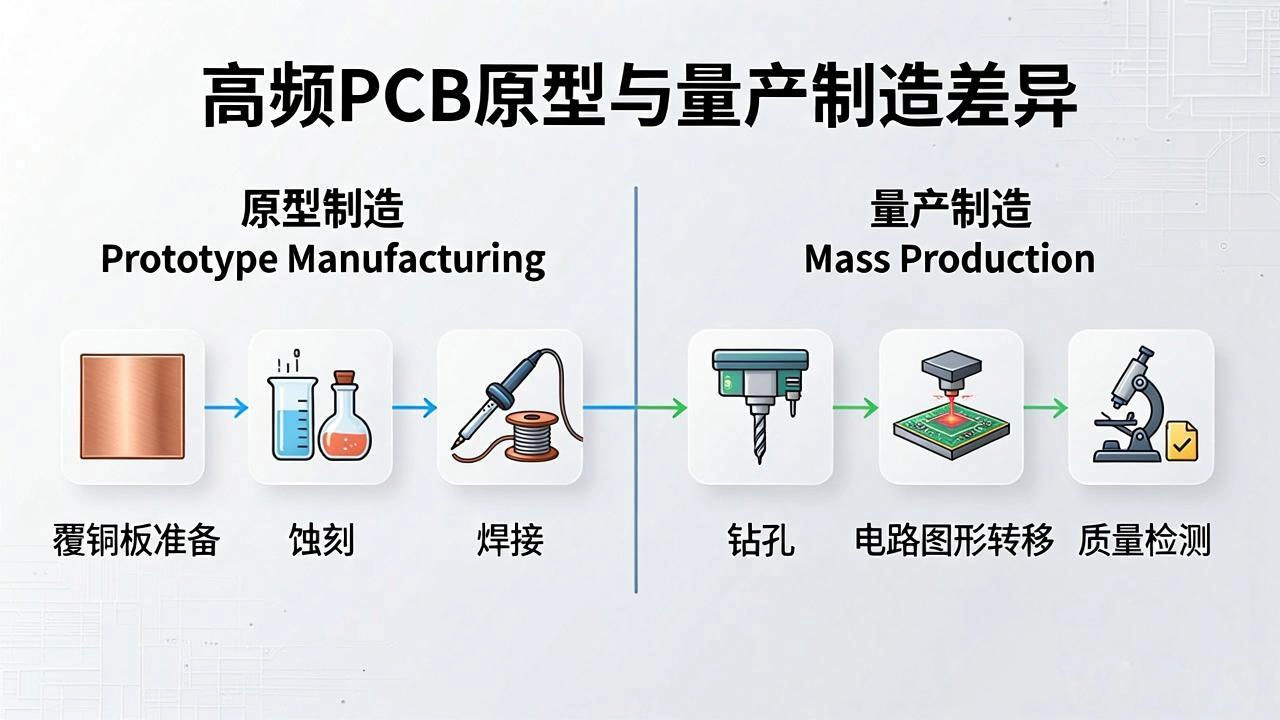
The fundamental difference lies in the end goal of each phase.
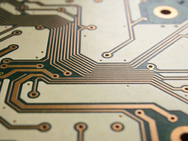
High-frequency PCBs rely on specialized dielectric materials (such as Rogers, Taconic, or Isola) rather than standard Fr-4. These materials have unique properties like low dielectric loss (Df) and stable dielectric constants (Dk).
During prototyping, manufacturers may use standard, readily available materials to ensure fast turnaround times. They might also use non-standard lamination parameters to get the board out the door quickly. However, in mass production, material specifications are strictly locked. High-frequency materials can exhibit slight variations in Dk and Df between different manufacturing batches. Mass production requires rigorous supply chain control and batch-testing to ensure that material variations do not cause impedance mismatches or signal attenuation.
A common pitfall in high-frequency PCB development is using a "prototype-only" stack-up.
In the prototype phase, engineers might adjust non-standard dielectric thicknesses or use specialized, small-batch lamination parameters to make the design work. While this achieves a passing test result in the lab, it is often unrepeatable on a mass production line. Mass production requires a fully optimized, standardized stack-up with fixed lamination temperatures, pressures, and times to guarantee layer-to-layer registration and consistent impedance.
High-frequency signals demand strict Impedance Control (e.g., 50Ω single-ended or 100Ω differential with ±5% tolerance).
During prototyping, a board might pass testing because the impedance sits right at the edge of the acceptable range (e.g., 48.5Ω to 51.5Ω), achieved through manual line-width adjustments by skilled engineers. In mass production, this narrow process window is a massive risk. Any minor fluctuation in etching or copper plating will push the impedance out of spec. Mass production fabrication requires designing for a wide, highly stable process window where impedance targets are comfortably met in the center of the tolerance band.
The testing methodologies also scale differently.
A successful high-frequency prototype is merely the first step. To transition smoothly to mass production, engineers must design with manufacturability in mind from day one. This means using production-grade stack-ups, validating material batch consistency, and ensuring impedance targets have a wide enough process window to accommodate automated manufacturing variations. Treating prototyping and mass production as distinct fabrication disciplines is the key to delivering reliable high-frequency electronics.
Common Pitfalls to Avoid During Your High Frequency PCB Prototype PhaseJune/18/2026

How to Prepare Gerber Files for a Successful High Frequency PCB PrototypeJuly/02/2026
The Benefits of Rapid High Frequency PCB PrototypingMay/29/2026
Why Impedance Control is Critical Even in High Frequency PCB PrototypesJuly/14/2026
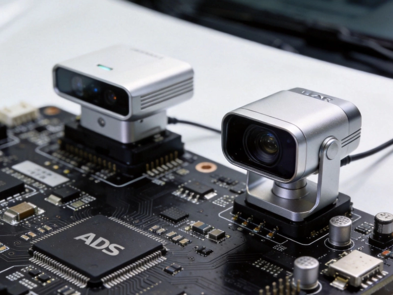
The Role of High Frequency PCB Applications in Autonomous Driving and ADASJuly/10/2026

Our Latest High Frequency PCB Capabilities for 6G ResearchMay/29/2026

High Frequency PCB Capabilities for Aerospace and Defense ApplicationsJuly/17/2026
Demystifying Impedance Control: Core High Frequency PCB KnowledgeJuly/09/2026