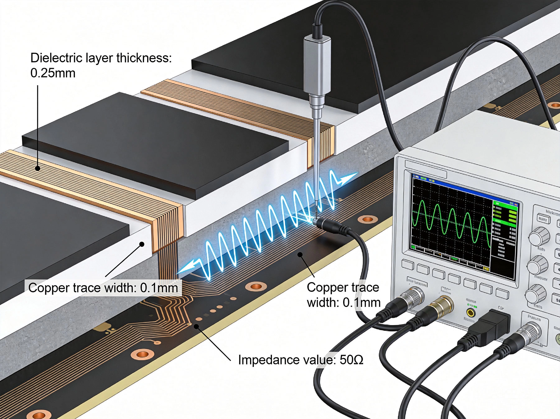
High Frequency Pcb Fabrication demands exceptional precision in material selection and process control. As signal speeds increase into the microwave and millimeter-wave frequencies, the Dielectric Constant (Dk) of PCB substrates becomes a critical parameter that directly impacts Signal Integrity, Impedance Matching, and overall circuit performance. Managing Dk tolerances represents one of the most significant challenges facing RF and Microwave Pcb manufacturers today.
When electrical signals propagate through transmission lines at high frequencies, the surrounding dielectric material interacts with the electromagnetic field in predictable ways. The Dielectric Constant determines the velocity of propagation and the effective capacitance between conductors. Variations in Dk, whether across the board or between production lots, translate directly into impedance deviations that can compromise circuit functionality.
The dielectric constant, also known as relative permittivity (εr), quantifies how an insulating material affects an electric field. In PCB applications, Dk values typically range from 2.0 for PTFE-based materials to 10.2 for high-Dk ceramic-filled laminates. Most standard Fr-4 materials exhibit Dk values between 4.2 and 4.8 at 1 GHz, though this value decreases with increasing frequency.
Dielectric constant is not a fixed value but varies with signal frequency. This phenomenon, known as dielectric dispersion, means that a material exhibiting Dk of 4.5 at 1 GHz may show Dk of 4.2 at 10 GHz. For wideband applications, this frequency dependence must be accounted for in design calculations and material selection.
Advanced high frequency laminates are engineered to minimize this frequency dependence, providing more predictable performance across wide frequency ranges. When specifying materials for 5G, radar, or Satellite Communications applications, engineers must obtain manufacturer data sheets showing Dk performance at multiple frequencies rather than relying on single-point specifications.
Material manufacturers specify Dk tolerances that typically range from ±0.5% for premium aerospace-grade materials to ±5% for standard commercial laminates. These tolerances directly affect the consistency of Controlled Impedance traces. A 50-ohm microstrip line fabricated on material with ±2% Dk tolerance will experience impedance variations of approximately ±1.5%, assuming all other process parameters remain constant.
High yield production of Rf Circuits requires much tighter effective tolerances. This necessitates not only careful material selection but also robust manufacturing processes that minimize additional sources of variation in copper roughness, substrate thickness, and trace geometry.
PCB substrate materials consist of resin systems reinforced with woven glass fibers or other reinforcements. The Dk of the resin differs significantly from the reinforcement material, creating composite structures with effective Dk values that depend on fiber weave density, resin content, and processing conditions. Woven glass reinforcement typically exhibits Dk values around 6.0, while epoxy resins range from 3.0 to 4.0.
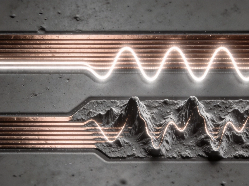
The fiberglass weave pattern introduces local Dk variations across the board surface. Areas with more glass fiber content show slightly higher effective Dk compared to resin-rich areas. This phenomenon, known as weave effect, becomes increasingly significant at higher frequencies where signal wavelengths approach the dimensions of weave openings.
Controlled variations in resin content provide one mechanism for adjusting laminate Dk. Higher resin content generally produces lower Dk, while increased filler loading increases Dk. During lamination, resin flow fills voids and encapsulates reinforcement, but non-uniform flow can create thickness and Dk variations across large panels.
Void content significantly impacts both Dk and Dissipation Factor. Even small voids (typically less than 1% by volume) can measurably affect electrical performance. Void formation becomes particularly problematic with low-flow prepreg materials and in areas with high circuit trace density.
hygroscopic nature of PCB substrates means they absorb moisture from the environment, with typical moisture content reaching 0.1% to 0.3% under normal conditions. Water has a Dk of approximately 80 at room temperature, so absorbed moisture significantly elevates the effective Dk of the substrate. A material absorbing 0.3% moisture might experience a 1-2% increase in Dk.
Moisture absorption also affects process parameters during drilling, plating, and assembly. Proper storage and handling procedures, including dry storage of sensitive materials and bake-out procedures before processing, help maintain consistent electrical properties.
The IPC TM-650 2.5.5.5 test method employs a clamped stripline resonator to measure Dk and Dissipation Factor (Df). This technique sandwiches the test material between two wide ground planes with a small coupling gap, creating a resonant structure that reveals material electrical properties through resonant frequency and quality factor measurements.
This method provides excellent accuracy (±0.5% for Dk) and is widely accepted as a standard specification method. However, it measures only the bulk material properties and cannot detect local variations across a panel or between different areas of a board.
Full sheet resonance testing provides a practical approach for measuring Dk variations across production panels. This non-destructive technique uses the entire panel as a resonant structure, with measured resonant frequencies related to material properties through established electromagnetic models. Variations across the panel surface become apparent through systematic mapping.
Many advanced PCB manufacturers implement automated full sheet resonance testing as part of their incoming material verification process. This data helps establish material consistency and identify panels that may require special handling or downstream testing adjustments.
Tdr Testing provides a practical correlation between material Dk and finished product impedance. By measuring the impedance of Controlled Impedance test coupons on each panel, manufacturers verify that impedance targets are achieved. While this method does not directly measure Dk, it provides excellent correlation to finished product performance.
Statistical analysis of impedance measurements across production runs enables estimation of effective process capability (Cpk) for impedance-controlled products. Cpk values above 1.33 are typically required for demanding RF applications, with values above 1.67 preferred for aerospace and defense contracts.
Several design approaches help mitigate the effects of fiberglass weave on signal performance. Using spread glass weaves reduces the periodic Dk variations that occur with standard weaves. Ceramic-filled PTFE materials without glass reinforcement provide the most uniform dielectric environment but at significantly higher cost.
Rotating the PCB design relative to the glass weave direction helps average out weave effects over longer trace segments. For critical signal paths, routing traces at 45-degree angles relative to the weave direction spreads the transition regions across more signal cycles, reducing the apparent magnitude of impedance discontinuities.
Symmetric stackups with balanced copper weights on opposite layers help maintain consistent overall board behavior during processing. Unequal copper densities cause differential shrinkage and movement during lamination, potentially introducing localized Dk variations in addition to dimensional changes.
For multi-layer boards, incorporating ground planes adjacent to signal layers provides electromagnetic shielding that reduces sensitivity to minor dielectric variations. The ground plane effectively averages the local Dk variations within its vicinity, providing more consistent effective permittivity for embedded transmission lines.
Designing circuits with wider acceptable impedance tolerances from the start provides manufacturing margin for Dk variations. While a 50-ohm target with ±1-ohm tolerance might seem ideal, specifying ±2-ohms or even ±3-ohms may enable more cost-effective manufacturing without sacrificing system performance.
Using differential routing instead of single-ended transmission lines provides inherent common-mode noise rejection that reduces sensitivity to impedance variations. The differential impedance depends primarily on trace spacing rather than absolute Dk values, making it more robust to material variations than single-ended lines.
Implementing incoming inspection for critical RF materials prevents production delays and yield losses from material-related issues. Testing each lot of material rather than relying on manufacturer certificates provides verification that the specific material received matches specifications. This becomes increasingly important when sourcing from multiple suppliers or distributors.
Material certificates typically report Dk values measured on representative samples using specific test methods. These values may not accurately represent the actual material in your production lot, particularly for materials with wide specification tolerances. Direct measurement of production material provides confidence that specifications will be met.
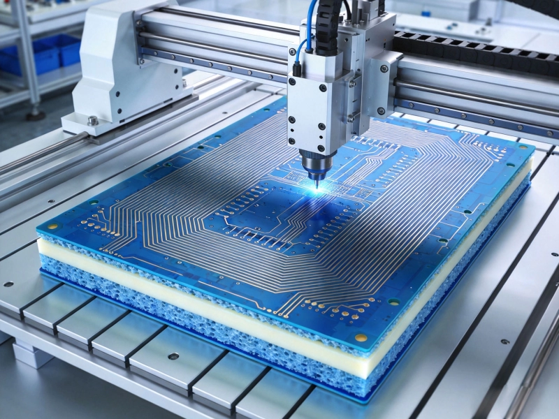
The lamination process directly affects final material Dk through effects on resin content, void formation, and cure state. Precise control of temperature, pressure, and time during lamination produces more consistent results than uncontrolled processes. Multi-stage lamination cycles with graduated pressure steps help ensure complete consolidation without excessive resin flow.
Post-lamination stress relief anneals can improve dimensional stability and reduce residual stress that might affect signal performance during thermal cycling. However, excessive post-cure can degrade electrical properties, particularly for filled PTFE materials that depend on specific cure conditions.
Chemical processing during etching and plating can affect surface smoothness and potentially influence the effective dielectric constant of thin substrates. Acid etching for copper removal introduces surface roughness that increases effective loss, particularly at very high frequencies where skin depth becomes small relative to surface irregularities.
Electroless copper plating adds a thin conductive layer that slightly modifies the effective dielectric environment for transmission lines. While typically negligible for standard constructions, this effect becomes more significant for ultra-thin dielectrics used in high-frequency applications.
PTFE-based laminates, including woven glass reinforced PTFE and ceramic-filled PTFE composites, provide the lowest dissipation factors and most stable Dk performance across wide frequency ranges. However, PTFE materials require special processing considerations including unique drill parameters, adhesive systems, and surface preparation treatments.
Ceramic-filled PTFE materials offer Dk values ranging from 2.9 to 10.2 with tolerances as tight as ±0.5% for premium grades. These materials are preferred for 5G infrastructure, Automotive Radar, and Satellite Communications where performance consistency is critical.
Hydrocarbon-based materials, often ceramic-filled, provide intermediate performance between Fr-4 and PTFE with significantly lower cost. These materials offer good Dk stability, low loss tangent, and processing characteristics similar to standard epoxy laminates. Dk tolerances of ±2% to ±3% are typical for commercial hydrocarbon products.
The improved thermal performance of hydrocarbon materials compared to FR-4 also benefits high-frequency applications that may experience significant self-heating from RF power dissipation. Thermal conductivity values of 0.5 to 1.0 W/mK help dissipate heat more effectively than standard substrates.
Modified epoxy systems with special fillers provide improved high-frequency performance compared to standard FR-4 while maintaining compatibility with conventional PCB processing. These materials represent a practical choice for applications where PTFE cost is prohibitive but improved electrical performance is still required.
Careful evaluation of modified epoxy materials is recommended, as performance can vary significantly between products marketed for high-frequency use. Accelerated life testing under temperature-humidity bias conditions helps identify materials that may degrade prematurely in demanding applications.
Implementing SPC on critical parameters including impedance, thickness, and Dk helps identify process drift before it affects production yields. Control charts tracking moving averages and ranges enable quick detection of process changes that might indicate material or equipment issues.
Cpk calculations for impedance measurements provide quantitative capability assessments that can be specified in quality agreements with PCB manufacturers. Regular capability studies verify that processes remain capable over time and across different equipment or shifts.
Maintaining traceability from finished boards back to specific material lots enables root cause analysis when field failures occur. Lot traceability also supports process optimization efforts by enabling correlation of finished product performance with specific material batches and manufacturing parameters.
Material certification packages should include Dk and Df test data, thickness measurements, copper foil specifications, and any special test results required for the application. For defense and aerospace applications, additional testing by independent laboratories may be required to meet contractual or regulatory requirements.
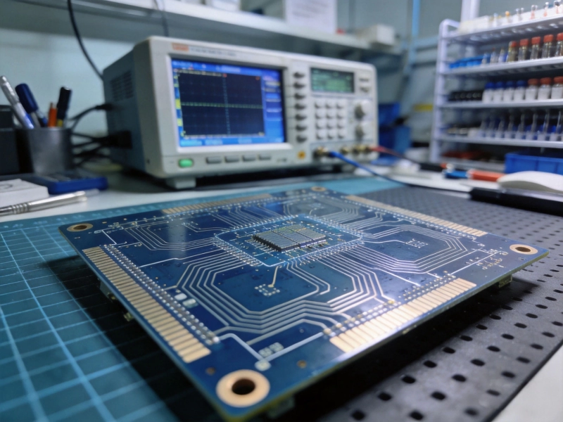
First-article inspection of prototype or initial production boards verifies that design intent translates into functional hardware. Network analyzer testing of S-parameters provides comprehensive characterization of RF performance including Insertion Loss, return loss, and Impedance Matching across the frequency range of interest.
Extended reliability testing under accelerated conditions helps identify any weaknesses in material selection or design before committing to full production. Temperature cycling, thermal shock, and biased humidity testing reveal failure modes that may not be apparent in short-term testing.
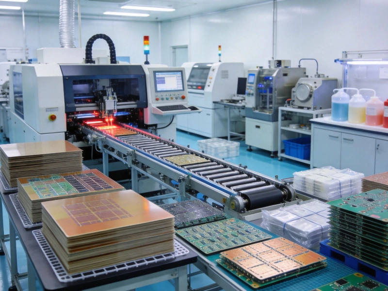
Not all PCB manufacturers in China possess the capabilities required for high-frequency applications. Key indicators of RF capability include specialized test equipment (network analyzers, TDR systems), controlled impedance testing on every production panel, material verification capabilities, and demonstrated experience with RF materials.
Requesting samples and capability qualifications from prospective suppliers provides direct evidence of manufacturing capability. Complex designs may benefit from first-article qualification programs that evaluate a limited production run before committing to volume manufacturing.
Clear communication of electrical and mechanical requirements helps ensure that suppliers understand expectations and can plan appropriate processes. Specifications should include target impedance values with tolerances, frequency range of operation, maximum acceptable loss, and any environmental or reliability requirements.
Material specifications should identify specific products by trade name and grade rather than generic material types. Different manufacturers' materials with similar descriptions may perform quite differently in actual production. Reference to specific datasheet parameters rather than just material families reduces ambiguity.
Managing dielectric constant tolerances in High Frequency Pcb Fabrication requires coordinated attention to material selection, design practices, manufacturing process controls, and quality verification. Success depends on understanding how Dk variations affect Signal Integrity and implementing appropriate countermeasures at each stage of product development and manufacturing.
While Dk tolerance management presents real challenges, modern materials and manufacturing processes enable reliable production of complex Rf Circuits to demanding specifications. Working closely with capable manufacturing partners and implementing appropriate design practices helps ensure that high-frequency products meet performance expectations while remaining cost-competitive.
The investment in proper High Frequency Pcb fabrication practices pays dividends through improved yield, reduced field failures, and enhanced customer satisfaction for RF and microwave applications across the rapidly expanding 5G, radar, and satellite communications markets.
Typical Dk tolerances for High Frequency Pcb Materials range from ±0.5% for premium aerospace-grade laminates to ±2-3% for commercial hydrocarbon materials. Standard FR-4 materials may have tolerances of ±5% or wider, making them unsuitable for most RF applications.
Dk variation directly affects the effective capacitance of transmission lines, which determines their Characteristic Impedance. A 2% Dk variation typically translates to approximately 1% impedance variation for microstrip lines. This can push traces outside specified tolerances if manufacturing margins are insufficient.
Applications above 1 GHz typically require attention to Dk tolerances, with increasingly stringent requirements at higher frequencies. At microwave frequencies (6 GHz and above), weave effect and material homogeneity become critical considerations alongside bulk Dk values.
While Dk cannot be directly measured on finished boards, impedance testing of controlled impedance coupons provides excellent correlation to effective Dk. Full sheet resonance testing can map Dk variations across panels without destroying the boards. Direct Dk measurement requires destructive testing of material samples.
Pcb Materials exhibit temperature-dependent Dk behavior characterized by their thermal coefficient of dielectric constant (TCDk), typically expressed in ppm/°C. High-frequency materials are engineered to minimize this temperature dependence. Thermal variations during operation can cause impedance drift in uncontrolled environments.
The Impact of Surface Roughness on High Frequency PCB Fabrication QualityJune/27/2026
High Frequency PCB Fabrication with Rogers and PTFE Materials: A Technical GuideJuly/16/2026
Laser Drilling and Microvias in Modern High Frequency PCB FabricationJuly/07/2026
Advanced High Frequency PCB Fabrication Techniques for Low Loss PerformanceMay/29/2026

High Frequency PCB Knowledge: How to Minimize Insertion Loss and ReflectionJuly/21/2026
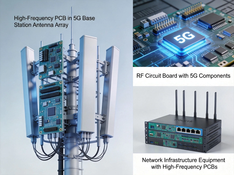
Top High Frequency PCB Applications in the 5G and Telecommunications IndustryJune/16/2026

Our Latest High Frequency PCB Capabilities for 6G ResearchMay/29/2026
Common Pitfalls to Avoid During Your High Frequency PCB Prototype PhaseJune/18/2026