Open Nav
When your dealing with high frequency circuits, Signal Loss is the enemy. Every decibel of attenuation matters, especially when you're pushing signals through the gigahertz range. Traditional PCB fabrication methods just ain't gonna cut it anymore - you need advanced techniques specifically designed to minimize loss and maintain Signal Integrity.
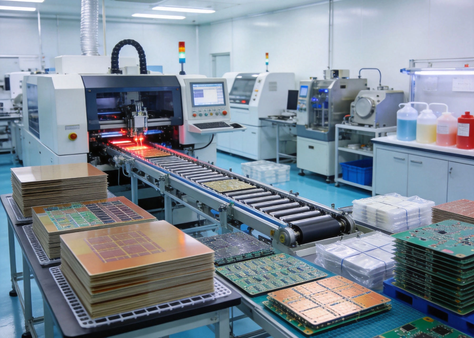
In this article, we gonna break down the cutting-edge fabrication techniques that make low loss high frequency PCBs possible. From material selection to precision etching processes, Impedance Control methods, and quality verification - we'll cover what actually works in real production environments. These aren't theoretical concepts; they're practical approaches that leading manufacturers use everyday.
Before diving into fabrication techniques, you gotta understand what causes Signal Loss in the first place. At high frequencies, signals behave differently than they do at lower frequencies. The PCB substrate, copper traces, and even the manufacturing process itself all contribute to signal degradation.
Types of signal loss in high frequency PCBs:
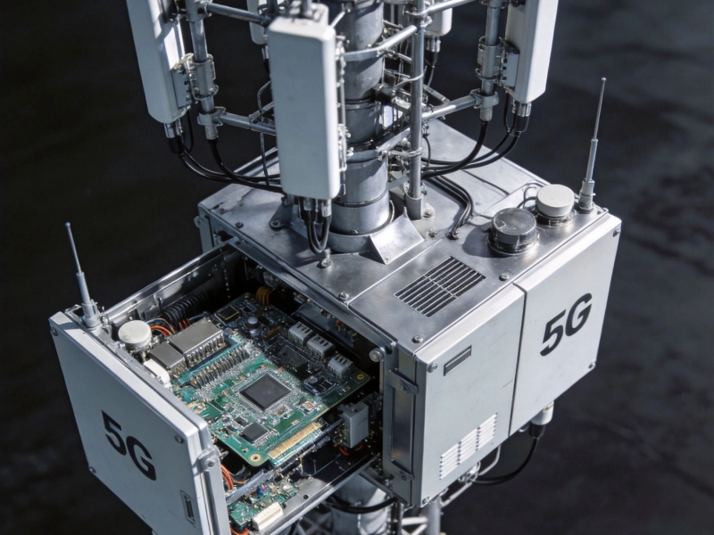
The combination of these losses determines your PCB's performance. In applications like 5G communications, radar systems, and high-speed data links, minimizing total loss is critical for system performance. That's why fabrication techniques have evolved specifically to address each type of loss.
The substrate material is the foundation of low loss performance. Standard FR-4 has a dielectric loss tangent (Df) around 0.02, which causes significant signal attenuation at frequencies above 1 GHz. For serious high frequency work, you need materials with much lower loss characteristics.
Popular low loss laminate options:
But here's the thing - selecting the right material ain't just about loss tangent. You also need to consider Dielectric Constant (Dk) stability, thermal properties, moisture absorption, and how the material behaves during fabrication. A material with amazing loss characteristics but terrible processability might end up causing more problems than it solves.
Beyond loss tangent, several material properties affect fabrication success and final performance:
I've seen designs fail because the selected material had great loss specs but poor thermal stability. The boards worked fine at room temperature but failed once they got hot in actual operation. Material selection has gotta account for real operating conditions.
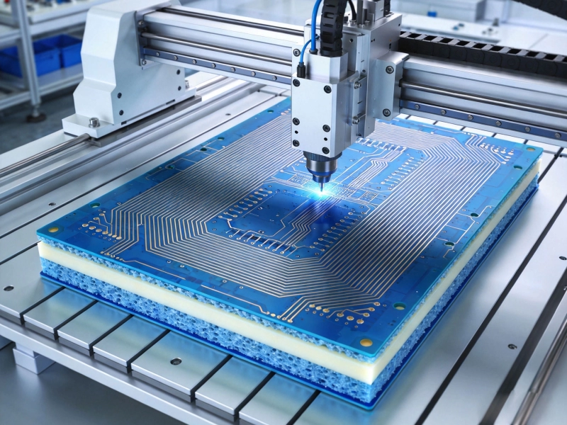
Trace geometry directly affects both impedance and signal loss. In standard PCB fabrication, etching tolerances might be ±10-20% of the nominal trace width. For high frequency applications, those tolerances are way too loose - you need precision etching that maintains tight dimensional control.
Advanced etching approaches:
For microstrip and stripline transmission lines, the trace width and copper thickness determine impedance. Standard 1 oz copper (35 μm) might work for some applications, but for higher frequencies, thinner copper often gives better results. Half-ounce (17.5 μm) or even quarter-ounce copper reduces conductor surface roughness effects that contribute to loss.
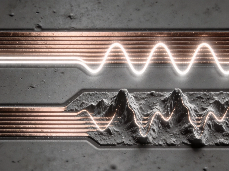
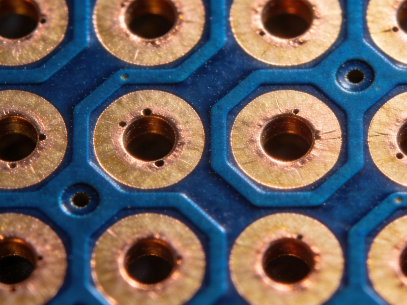
At high frequencies, current flows primarily on the conductor surface (Skin Effect). The Copper Surface Roughness directly impacts conductor loss - rougher surfaces increase effective resistance. Standard PCB copper has roughness around 2-5 μm, which becomes problematic above a few gigahertz.
Low loss surface treatments:
The tradeoff with smoother copper is adhesion. Very smooth surfaces might not bond well to the substrate. Advanced fabrication techniques balance smoothness with adhesion through optimized substrate surface preparation and foil treatment processes.
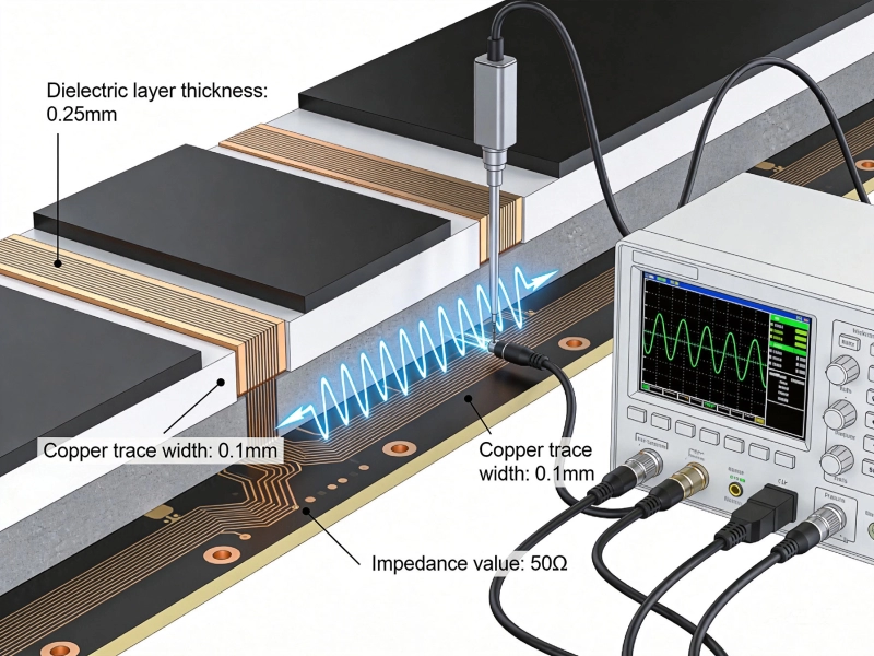
Impedance depends on multiple dimensional factors: trace width, trace thickness, substrate thickness, and dielectric constant. Maintaining impedance within tight tolerances requires controlling all these variables during fabrication.
Stack-up tolerance control:
For impedance tolerances of ±5% or tighter, you need fabrication processes that can maintain dimensional tolerances at similar levels. Standard fabrication might give ±10% impedance tolerance; achieving ±5% requires everything from material selection to final inspection to be optimized.
Test coupons - small sections of the PCB that contain representative transmission line structures - let you verify impedance without measuring actual circuit traces. Advanced fabrication includes properly designed test coupons that accurately reflect production trace characteristics.
Test coupon design considerations:
I recommend including test coupons on every High Frequency Pcb panel. They let you verify that fabrication achieved target impedance before the boards go into assembly. If the coupons fail impedance testing, you can catch the problem early instead of discovering it after expensive components are soldered onto defective boards.
Vias - the holes that connect different PCB layers - can significantly affect high frequency performance. Each via introduces impedance discontinuity and adds parasitic inductance and capacitance. The fabrication process for vias matters just as much as the design.
Via-related loss mechanisms:
Advanced fabrication techniques address these issues through back-drilling (removing via stubs), controlled via diameters, and optimized via plating. For really critical signals, some manufacturers use laser-drilled microvias that offer better high frequency performance than mechanically drilled holes.
Back-drilling removes the unused portion of vias to eliminate stub resonance effects. It's a precision operation that requires careful control - drilling too deep damages the board, drilling too shallow leaves stubs that still cause problems.
Back-drilling considerations:
Not every fabrication house can do back-drilling well. It requires specialized equipment and experienced operators. When selecting a fabrication partner for high frequency work, verify their back-drilling capability and ask about their process controls.
You can't just assume fabrication succeeded - you need actual electrical testing to verify low loss performance. Advanced fabrication facilities use specialized test equipment designed for high frequency measurements.
Key electrical tests:
For production boards, test coupon measurements might be sufficient. For prototype or first-article boards, full electrical testing of actual signal paths gives more confidence. The level of testing depends on your application requirements and how much risk you can tolerate.
Physical dimensions directly affect electrical performance, so dimensional inspection is critical. Advanced fabrication uses automated optical inspection (AOI) and coordinate measuring machines (CMM) to verify dimensions.
Dimensional verification points:
Documentation is just as important as measurement. Good fabrication facilities provide detailed reports showing actual measurements versus specifications. This documentation helps you understand whether fabrication met requirements and gives data for failure analysis if problems arise later.
Not every Pcb Manufacturer can deliver low loss high frequency boards. When selecting a fabrication partner, you need to evaluate their capabilities specifically for advanced high frequency work.
Questions to ask potential partners:
The right partner should have experience with materials beyond standard FR-4, precision process controls, and appropriate test capabilities. They should also be willing to work with your design team to ensure the layout supports their fabrication capabilities.
Putting it all together, successful low loss High Frequency Pcb fabrication requires:
None of these elements stands alone - they all interact. Material choice affects etching requirements. Trace geometry affects impedance. Via design affects overall Signal Integrity. Successful fabrication means getting all these factors right together.
Low loss high frequency PCB fabrication is specialized work that requires both knowledge and capability. The techniques described here are proven approaches that leading manufacturers use for demanding RF and microwave applications.
Need expert guidance for your high frequency PCB project? Work with fabrication specialists who understand these advanced techniques and can deliver boards that meet your loss and impedance requirements.
Advanced fabrication techniques make low loss high frequency PCBs possible, but they require coordinated effort across material selection, processing methods, and quality verification. Understanding these techniques helps you design better boards and work more effectively with fabrication partners.
The key insight is that low loss ain't just about selecting fancy materials - it's about the whole fabrication process being optimized for high frequency performance. From precision etching to impedance control, via optimization to surface roughness management, every fabrication step affects final performance.
When you approach high frequency PCB fabrication with this understanding, you can make informed decisions about materials, processes, and manufacturing partners. You can design layouts that support fabrication capabilities and specify requirements that manufacturers can actually deliver. That's how you get high frequency boards that perform reliably in demanding applications.
Q: What loss tangent value is considered "low loss" for high frequency PCBs?
A: Generally, materials with Df below 0.005 are considered low loss. For demanding applications above 10 GHz, materials with Df below 0.002 are typically used. Ultra-low loss applications may require Df below 0.001.
Q: How does copper thickness affect high frequency signal loss?
A: At high frequencies, Skin Effect means current flows near the conductor surface. Thinner copper can have smoother surfaces and less roughness-related loss. However, very thin copper may have higher DC resistance, so the optimal thickness depends on your specific frequency range and application.
Q: What impedance tolerance is achievable with advanced fabrication?
A: Standard fabrication typically achieves ±10% impedance tolerance. Advanced processes with tight dimensional control can achieve ±5% routinely. With exceptional process control and design optimization, ±3% or even tighter tolerances are possible for critical signal paths.
Q: Why is back-drilling important for high frequency PCBs?
A: Via stubs - the unused portion of through-hole vias - act as resonant elements at specific frequencies. This stub resonance causes signal reflection and loss. Back-drilling removes these stubs, eliminating resonance effects and improving signal integrity for high frequency paths.
Q: Can standard fabrication facilities handle advanced high frequency materials?
A: Some can, but many standard facilities lack experience with materials like Rogers, Taconic, or specialized Isola laminates. These materials have different processing requirements than FR-4. Always verify that your fabrication partner has specific experience with your selected materials before committing to production.
High Frequency PCB Fabrication: Managing Dielectric Constant (Dk) TolerancesJune/09/2026
The Impact of Surface Roughness on High Frequency PCB Fabrication QualityJune/27/2026
High Frequency PCB Fabrication with Rogers and PTFE Materials: A Technical GuideJuly/16/2026
Laser Drilling and Microvias in Modern High Frequency PCB FabricationJuly/07/2026

Our Latest High Frequency PCB Capabilities for 6G ResearchMay/29/2026
Why Impedance Control is Critical Even in High Frequency PCB PrototypesJuly/14/2026
SMT vs. THT: Assembly Techniques for High Frequency PCBsJuly/03/2026
Top High Frequency PCB Applications in the 5G and Telecommunications IndustryMay/29/2026