Open Nav
5G ain't just faster 4G - it's a whole new approach to wireless communications that demands fundamentally different hardware. The high frequency PCBs that power 5G systems operate at frequencies, power levels, and integration densities that previous generations never needed. From massive MIMO antenna arrays to millimeter-wave front-end modules, the PCB technology behind 5G represents significant advances in RF engineering.
In this article, we'll explore the major High Frequency Pcb applications that make 5G and modern telecommunications possible. We'll look at base station infrastructure, mobile device designs, and emerging applications that push PCB technology further. For each application area, we'll discuss the specific PCB requirements, design challenges, and technology approaches that enable performance. If you're working in telecommunications or just want to understand how 5G hardware actually works, this overview covers what matters.
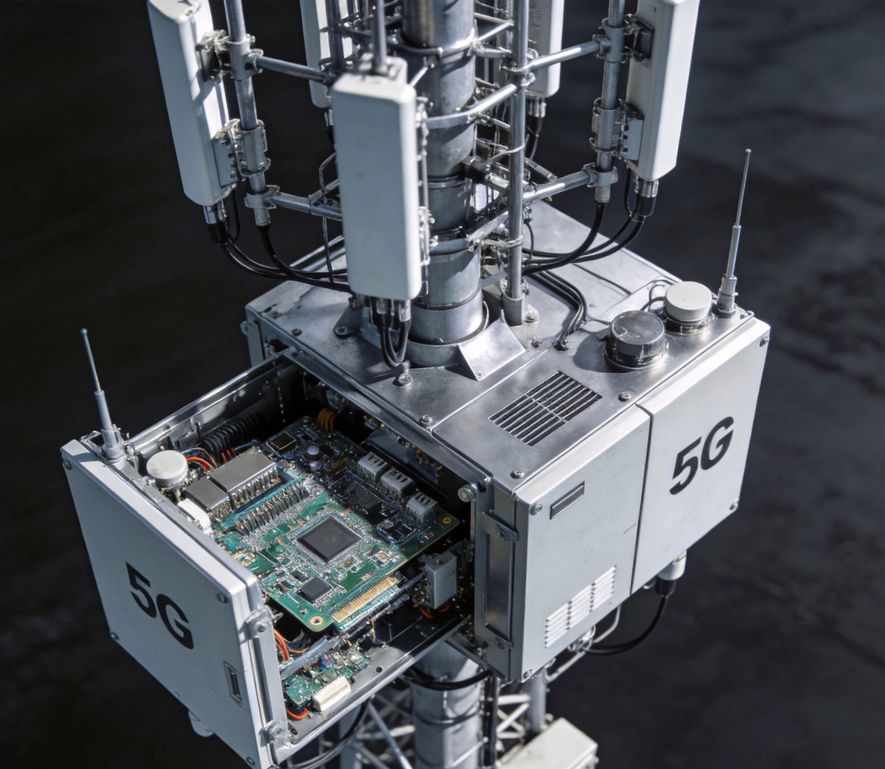
Base stations are where 5G signals originate and terminate. The RF front-end - the circuitry that generates, amplifies, filters, and routes radio signals - depends entirely on high frequency PCBs. These boards handle everything from signal generation at the transmitter to signal reception and processing at the receiver.
Base station RF front-end functions:
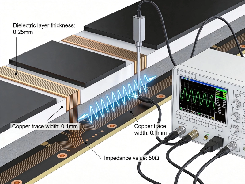
The PCBs supporting these functions operate at frequencies from sub-6 GHz bands up to millimeter-wave bands (24-40+ GHz). They handle significant power levels - macro base stations might transmit hundreds of watts, requiring PCBs designed for both Signal Integrity and thermal management.
Massive MIMO is a defining 5G technology. Traditional base stations used a few antennas; massive MIMO arrays use 64, 128, or even more antenna elements. Each element needs its own RF path, creating PCB designs with unprecedented complexity and integration density.
Massive MIMO PCB requirements:
Massive MIMO PCBs represent some of the most complex RF designs ever mass-produced. They combine high frequency signal paths, digital control circuits, power distribution, and thermal management in densely packed assemblies. Design and fabrication challenges include maintaining impedance across hundreds of transmission lines, controlling thermal effects on signal performance, and achieving reproducible phase alignment between array elements.
5g Base Station power amplifiers are more complex than previous generations. Multi-band operation, wider bandwidth, and higher efficiency requirements drive sophisticated amplifier designs that depend on specialized PCB approaches.
Power amplifier PCB considerations:
Power amplifier PCBs often use thick copper for thermal management, specialized laminate materials for low loss, and carefully designed impedance transitions between amplifier stages. The integration of multiple amplifiers for different frequency bands creates complex board layouts that must maintain performance across varied operating conditions.
5G millimeter-wave bands - roughly 24-40 GHz depending on region - represent new territory for mass telecommunications. These frequencies offer huge bandwidth but present significant engineering challenges. PCBs for mmWave applications need specialized designs that go beyond traditional RF approaches.
mmWave PCB challenges:
At mmWave frequencies, loss becomes critical. Standard Pcb Materials would attenuate signals so severely that useful range becomes impractical. mmWave PCBs typically use specialized materials like Rogers RO3000 series or similar ultra-low loss laminates, with precision fabrication maintaining tight dimensional tolerances.
mmWave antennas are small enough to integrate directly on PCBs rather than using separate antenna components. This integration reduces interconnect loss and enables precise array positioning, but creates complex PCB designs that combine antenna elements with feed networks and Rf Electronics.
Integrated Antenna Pcb features:
These integrated antenna PCBs operate at frequencies where trace geometry directly affects antenna performance. Element dimensions, spacing, and feed network characteristics all influence radiation patterns, bandwidth, and efficiency. The integration density pushes fabrication capabilities, requiring precise control of multiple PCB layers and structures.
mmWave phased arrays - antenna systems that electronically steer beams without physical movement - depend on sophisticated PCB assemblies. Each antenna element needs its own signal path with phase control, creating dense RF interconnect structures.
Phased array PCB architecture:
Phased array PCBs for telecommunications need to achieve beam steering accuracy while maintaining performance across the full frequency band. The phase relationships between elements must be controlled precisely, requiring PCB fabrication that delivers reproducible signal paths. Temperature variations, fabrication tolerances, and material variations all affect phase accuracy.
Modern smartphones are essentially sophisticated RF systems with computing and display added. 5G smartphones support multiple frequency bands, multiple antenna configurations, and complex RF signal routing - all constrained by severe size limitations. The PCB designs enabling these capabilities represent remarkable engineering achievement.
Smartphone Rf Pcb requirements:
Smartphone RF PCBs typically use multilayer designs with Rf Circuits on outer layers, digital processing in inner layers, and ground planes separating RF and digital sections. The RF sections use appropriate laminate materials while keeping overall cost manageable for consumer products.
Smartphone RF front-ends have evolved into sophisticated module assemblies. A single module might contain power amplifiers, low-noise amplifiers, filters, switches, and duplexers for multiple frequency bands. These modules depend on specialized PCBs designed for dense RF integration.
RF module PCB features:
These module PCBs often use Advanced Substrate Materials rather than traditional PCB laminates. The integration density approaches semiconductor packaging complexity, requiring fabrication capabilities beyond standard Pcb Manufacturing. Module suppliers have developed specialized processes for these demanding applications.
mmWave 5G smartphones integrate antennas directly with Rf Electronics rather than using separate antenna components. Antenna-in-package (AiP) designs place antenna elements within the IC package itself. Antenna-on-PCB designs fabricate antenna structures directly on the phone's main PCB. Both approaches create new PCB design challenges.
Integrated antenna approaches:
These integrated designs reduce the interconnect distance between antennas and RF electronics, critical for mmWave frequencies where even small interconnects add significant loss. The PCB design must accommodate antenna structures while maintaining overall phone architecture and managing interference between systems.
5G networks use many small cells in addition to macro base stations. These small cells - compact base stations serving limited coverage areas - need sophisticated RF PCBs despite their smaller size. The economics of dense deployment require cost-effective designs that still deliver required performance.
Small cell PCB requirements:
Small cell PCBs balance performance requirements against cost constraints. They typically use moderately priced materials rather than the ultra-low loss laminates used in macro base stations. Design optimization focuses on achieving adequate performance with practical cost for large-scale deployment.
Distributed antenna systems (DAS) spread antenna coverage throughout buildings or venues using remote antenna units connected to centralized processing. The remote units contain RF PCBs that interface between the distribution network and the antenna elements.
DAS remote unit PCBs:
DAS PCBs need to maintain performance despite the constraints of remote deployment. Limited power availability, varied environmental conditions, and cost sensitivity for multi-site deployment all affect PCB design approaches.
Satellite Communications - both traditional GEO satellites and emerging LEO constellations - depend on high frequency PCBs for ground terminals and satellite payloads. These applications have unique requirements driven by space environment constraints and performance demands.
Satellite communication PCB requirements:
Satellite payload PCBs often use specialized materials for stability and reliability. Ground terminal PCBs have less extreme environmental requirements but still need reliable operation for extended periods. Both applications require performance optimization for specific satellite communication bands.
Satellite ground terminals for modern high-throughput systems need sophisticated RF PCBs. User terminals for LEO internet services, VSAT systems for enterprise communications, and gateway terminals for network backhaul all require High Frequency Pcb designs.
Ground terminal PCB applications:
These terminal PCBs operate at frequencies ranging from traditional satellite bands (C, Ku, Ka) to newer high-throughput allocations. The designs balance performance requirements against practical constraints like terminal size, power consumption, and production cost.
Wireless backhaul - using microwave links to connect base stations to the core network - depends on high frequency PCBs for both ends of the link. These systems operate at frequencies from traditional microwave bands (6-38 GHz) up to E-band (70-80 GHz) for high-capacity links.
Microwave backhaul PCB requirements:
Backhaul PCBs need to achieve high performance while operating in outdoor environments for years without maintenance. Reliability and environmental tolerance are key design considerations alongside RF performance.
E-band backhaul (70-80 GHz) offers very high capacity for dense network deployments. These systems operate at frequencies where specialized PCB approaches are essential. The millimeter-wave technology needs Ultra-low Loss Materials and precision fabrication.
E-band PCB challenges:
E-band PCBs represent some of the most demanding telecommunications applications. The combination of high frequency, outdoor deployment, and reliability requirements drives specialized design and fabrication approaches.
6g Research is already pushing PCB technology further. Anticipated frequencies extending into sub-THz range (100-300 GHz) will require new materials, fabrication techniques, and design approaches. Research platforms need PCBs that can operate at frequencies beyond current telecommunications limits.
6g Research Pcb challenges:
6g Research PCBs are still largely in development phase. Material suppliers, fabrication specialists, and research teams are collaborating to develop capabilities that will enable sub-THz telecommunications hardware.
Future telecommunications systems may integrate sensing functions - using the same RF hardware for communication and environmental sensing. This integration creates PCB designs that support both communication performance and sensing accuracy.
Integrated sensing/communication PCB considerations:
This emerging application area combines telecommunications PCB expertise with radar system design knowledge. The integration creates new design challenges that are being explored in research and early development programs.
Different telecommunications applications need different Pcb Materials. The selection balances performance requirements against cost constraints and fabrication practicality.
Material recommendations by application:
Material selection should consider total system economics. Using ultra-low loss materials in low-margin applications might not be economically viable. Conversely, using inadequate materials in high-performance applications leads to system failures that cost far more than material upgrades.
Telecommunications PCB fabrication ranges from standard capabilities to highly specialized processes. Application complexity determines fabrication requirements.
Fabrication capability tiers:
Selecting fabrication partners requires matching their capabilities to application requirements. Not all PCB fabricators can handle high frequency telecommunications boards effectively. Experience with specific materials and frequency ranges matters for achieving reliable performance.
Telecommunications applications represent some of the most demanding high frequency PCB work. Successful development requires expertise in RF design, material selection, fabrication processes, and application-specific requirements.
What telecommunications PCB development needs:
If your telecommunications project needs high frequency PCB development, finding partners with relevant experience accelerates success. Understanding the application landscape - which we've covered in this article - helps you communicate requirements effectively and evaluate proposed solutions.
We work with telecommunications developers on base station hardware, mobile device RF, backhaul systems, and emerging applications. Our experience across these application areas helps teams navigate design challenges, material selection, and fabrication requirements.
Contact us to discuss your telecommunications PCB project: We'll review your application requirements, frequency needs, and production plans to develop approaches that work for your specific situation.
High frequency PCBs enable 5G and modern telecommunications across a remarkable range of applications. From macro base stations handling hundreds of watts to smartphone RF modules fitting into millimeter-scale volumes, the PCB technology supporting telecommunications has evolved dramatically.
Each application area we've covered - base station infrastructure, millimeter-wave systems, mobile devices, distributed antenna systems, Satellite Communications, and network backhaul - has specific PCB requirements driven by performance needs, environmental constraints, and economic realities. Understanding these requirements helps designers and developers create PCB solutions that work reliably in demanding telecommunications environments.
The evolution continues. 6G research, integrated sensing applications, and new deployment architectures will push PCB technology further. The foundational capabilities developed for 5G - precision fabrication, advanced materials, complex integration - provide the basis for future advances. Telecommunications PCB development combines RF expertise with practical engineering, balancing performance against constraints to enable the wireless connectivity that modern society depends on.
Q: What frequencies do 5G PCBs typically operate at?
A: 5G PCBs operate across multiple frequency ranges: sub-6 GHz bands (traditional cellular frequencies), millimeter-wave bands (24-40 GHz depending on region), and supporting frequencies for backhaul and satellite links. Different frequency ranges need different PCB materials and design approaches.
Q: How do mobile device PCBs differ from base station PCBs?
A: Mobile device PCBs have severe size constraints, use cost-optimized materials, and integrate massive functionality into compact volumes. Base station PCBs have larger form factors, use higher-performance materials, handle much higher power levels, and prioritize performance over cost optimization.
Q: What materials are used for millimeter-wave telecommunications PCBs?
A: Millimeter-wave PCBs typically use ultra-low loss materials like Rogers RO3000 series (Df as low as 0.0013) or similar specialized laminates. Standard materials would cause excessive Signal Loss at mmWave frequencies, severely limiting system performance and range.
Q: How does massive MIMO affect PCB design complexity?
A: Massive MIMO arrays with 64-128 antenna elements require PCBs with dense RF integration, precise phase control, and complex signal routing. Each antenna element needs its own RF path, creating boards with hundreds of transmission lines that must maintain impedance and phase accuracy.
Q: Can the same PCB fabricator handle all telecommunications applications?
A: Not necessarily. Different applications require different fabrication capabilities. Mobile device PCBs might use standard high-volume processes, while mmWave base station boards need specialized precision fabrication. Fabrication partners should be matched to specific application requirements.
Pushing the Limits: Our Latest High Frequency PCB Capabilities for 6G ResearchJune/11/2026
From Prototype to Mass Production: Scaling with a Reliable High Frequency PCB ManufacturerJuly/13/2026
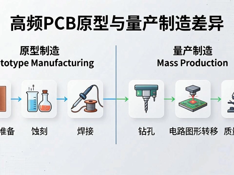
High Frequency PCB Prototype vs. Mass Production: Key Differences in FabricationJune/05/2026

High Frequency PCB Capabilities for Aerospace and Defense ApplicationsJuly/17/2026
High Frequency PCB Fabrication: Managing Dielectric Constant (Dk) TolerancesJune/09/2026
Essential High Frequency PCB Knowledge for Hardware Engineers and DesignersMay/29/2026
The Challenges of High Frequency PCB Assembly: Handling Sensitive ComponentsMay/29/2026
The Role of High Frequency PCB Applications in Autonomous Driving and ADASJuly/10/2026