Open Nav
High Frequency Pcb design represents one of the most challenging and specialized areas of Electronics Engineering. As wireless technologies, high-speed digital systems, and RF applications continue to advance, hardware engineers and designers must develop deep understanding of High Frequency Pcb principles to ensure reliable performance. Unlike standard digital PCB design, high frequency circuits require careful attention to electromagnetic theory, transmission line behavior, and material properties. Whether you're designing Rf Circuits for 5G applications, high-speed digital interfaces, or microwave systems, mastering high frequency PCB knowledge is essential for creating robust, high-performance electronic products. This comprehensive guide covers the fundamental concepts, design considerations, and practical techniques that every hardware engineer needs to know for successful high frequency PCB development.
The foundation of High Frequency Pcb Design lies in understanding how signals behave differently at higher frequencies. At low frequencies, signals propagate almost instantaneously, and PCB traces can be treated as simple conductors. However, as frequency increases beyond approximately 50-100 MHz, signal wavelengths become comparable to trace lengths, and wave propagation effects become significant. This transition marks the point where traditional circuit theory breaks down and transmission line theory becomes necessary for accurate design and analysis.
In the high frequency regime, several phenomena that engineers can ignore at lower frequencies become critically important. Signal reflections occur when impedance mismatches cause portions of the signal to bounce back toward the source, potentially causing Signal Integrity issues. Crosstalk between adjacent traces increases as electromagnetic coupling becomes stronger at higher frequencies. Dielectric losses increase with frequency, causing signal attenuation. These effects can lead to timing violations, signal distortion, increased bit error rates, and overall system unreliability if not properly addressed in the design phase.
The concept of wavelength is fundamental to High Frequency Pcb Design. The wavelength (λ) of a signal is determined by the formula λ = c/f, where c is the speed of light and f is frequency. However, on PCBs, the effective propagation velocity is slower due to the Dielectric Constant of the PCB material. Engineers typically use the rule that when a trace length exceeds 1/10 or 1/20 of the signal wavelength, it must be treated as a transmission line rather than a simple conductor. For example, at 1 GHz, the wavelength in Fr-4 material is approximately 6 inches, so traces longer than 0.3-0.6 inches require transmission line treatment.
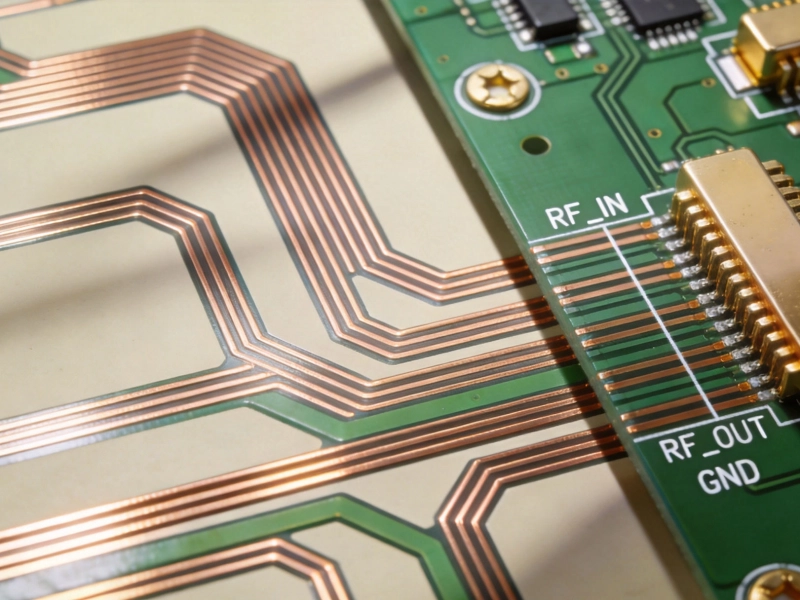
Impedance Control is perhaps the single most important aspect of high frequency PCB design. In transmission line theory, the Characteristic Impedance (Z0) of a trace is determined by its physical geometry and the dielectric properties of the PCB material. For high frequency signals, maintaining consistent impedance throughout the signal path is critical to preventing reflections and ensuring Signal Integrity. Common impedance values include 50Ω for RF systems and microwave applications, 75Ω for video and telecommunications, and 100Ω for differential pairs in high-speed digital interfaces.
Several transmission line configurations are commonly used in high frequency PCB design:
Calculating Characteristic Impedance requires considering multiple factors including trace width, trace thickness, dielectric thickness, Dielectric Constant, and the geometry of ground planes. Engineers typically use specialized impedance calculators or electromagnetic simulation software to determine the correct trace dimensions for their target impedance. Manufacturing tolerances must also be considered, as variations in trace width, dielectric thickness, and dielectric constant can affect the actual impedance achieved. For critical applications, impedance testing and Controlled Impedance fabrication processes are essential.
The choice of PCB material significantly impacts high frequency circuit performance. While standard Fr-4 material is adequate for many applications up to a few gigahertz, specialized high frequency materials become necessary for demanding RF and microwave applications above 3-5 GHz. Key material properties that affect high frequency performance include dielectric constant (Dk), Dissipation Factor (Df), thermal conductivity, and moisture absorption.
Dielectric constant determines how quickly signals propagate through the material and affects impedance calculations. High frequency materials typically have lower and more stable dielectric constants compared to FR-4. FR-4 has a dielectric constant around 4.0-4.5 at 1 MHz, but this value decreases with frequency and can vary between different laminate batches. High frequency materials like Rogers RO4003C have a more stable dielectric constant around 3.55 with minimal variation across frequency and temperature.
Dissipation Factor, also called loss tangent, indicates how much signal energy is lost as heat as it propagates through the dielectric material. Lower dissipation factor means lower Signal Loss, which is critical for high frequency applications where signal attenuation can become significant. FR-4 typically has a dissipation factor around 0.02 at 1 GHz, while high frequency materials can have values as low as 0.001-0.002. This dramatic difference in loss characteristics makes specialized materials essential for millimeter-wave applications above 30 GHz.
Popular High Frequency Pcb Materials include:
When selecting Pcb Materials for high frequency applications, engineers must consider not only electrical performance but also manufacturability, cost, availability, and thermal requirements. Working closely with PCB fabricators early in the design process helps ensure material compatibility and manufacturability.
Signal integrity (SI) and electromagnetic interference (EMI) are critical concerns in high frequency PCB design. Poor signal integrity leads to timing violations, data corruption, and system failures, while EMI can cause regulatory compliance issues and interfere with other electronic systems. Addressing these challenges requires careful attention to PCB layout, grounding, and shielding practices.
Grounding is one of the most important aspects of high frequency PCB design. A solid, continuous ground plane provides a low-impedance return path for signals, reduces electromagnetic radiation, and helps maintain Impedance Control. High frequency designs typically use ground planes on multiple layers connected with numerous vias to minimize ground impedance and prevent ground bounce. The concept of return current path is particularly important—high frequency return currents preferentially flow in the ground plane directly underneath the signal trace, and any discontinuities in this path can cause impedance variations and increased EMI.
Vias represent potential impedance discontinuities in high frequency designs. The transition between layers introduces additional parasitic inductance and capacitance that can affect signal integrity. For critical high frequency signals, techniques like via stitching (placing multiple ground vias around signal vias), back-drilling (removing unused via stubs), and blind/buried vias can help minimize via effects. In extreme cases, edge-plating or coaxial via structures may be used for the most demanding applications.
Crosstalk reduction is another critical consideration for high frequency designs. Crosstalk occurs when signals couple electromagnetically between adjacent traces, causing unwanted signal transfer. Techniques to reduce crosstalk include increasing spacing between traces, using ground traces or ground planes between signals, minimizing parallel run lengths, and using differential signaling where appropriate. For very high frequency designs, 3D electromagnetic simulation can help identify and mitigate crosstalk issues before fabrication.
Shielding techniques become important for sensitive Rf Circuits and to prevent EMI emission. Ground planes, shielding cans, and proper partitioning of analog, digital, and RF sections help contain electromagnetic energy. High frequency circuits often benefit from dedicated shielding cans or metal covers that prevent external interference and reduce emissions. Partitioning the PCB into separate zones for different functional areas helps prevent noise coupling between circuit blocks.
Successful high frequency PCB design requires attention to numerous practical details that can significantly impact performance. Following established best practices and design guidelines helps ensure manufacturable, reliable designs that meet performance requirements. These practices have been developed through decades of experience in high frequency circuit design and represent proven approaches to common challenges.
Trace routing guidelines are fundamental to high frequency PCB design:
Component Placement and selection significantly affect high frequency performance:
Manufacturing considerations are essential for ensuring that high frequency designs can be fabricated reliably:
Simulation and analysis tools are invaluable for high frequency PCB design:
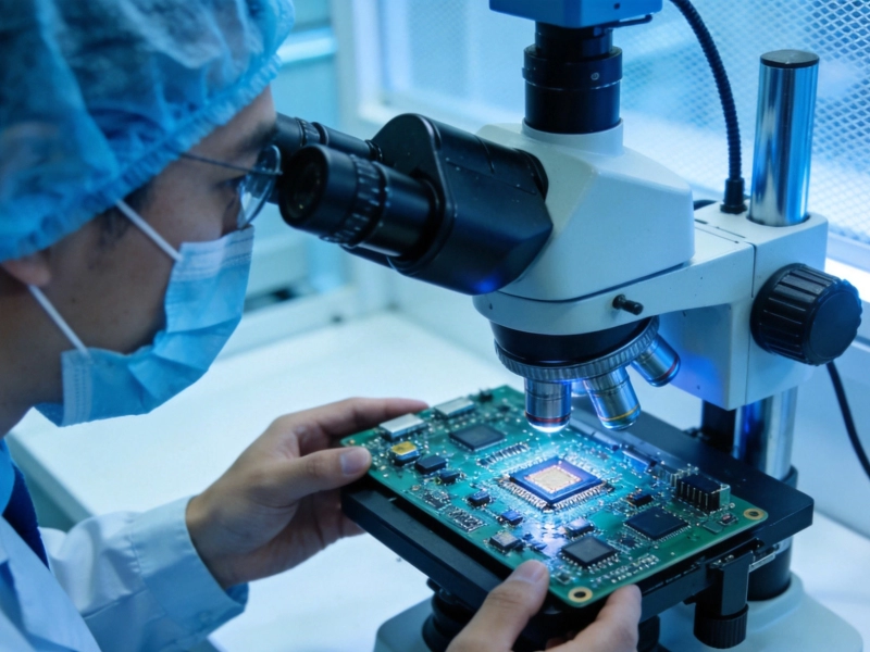
Testing and validation are critical steps in high frequency PCB development that ensure designs meet performance requirements and are ready for production. High frequency circuits require specialized test equipment and measurement techniques beyond those used for standard digital circuits. Proper testing methodology helps identify design issues early, validate performance, and ensure reliability in production.
Time-domain reflectometry (TDR) is essential for impedance verification. TDR measurements allow engineers to measure the characteristic impedance of transmission lines and identify impedance discontinuities along signal paths. Modern TDR instruments provide detailed impedance profiles that reveal problems like via stubs, layer transitions, and impedance mismatches. Tdr Testing should be performed on prototype boards to verify that the fabricated impedance matches the design intent.
Network analysis provides comprehensive characterization of high frequency circuits. Vector network analyzers (VNAs) measure S-parameters (scattering parameters) that characterize how RF signals interact with circuits. S-parameter measurements reveal Insertion Loss, return loss, VSWR, phase response, and other critical parameters. For differential signals, differential S-parameter measurements characterize differential mode and common mode behavior. Network analysis is essential for RF circuits, filters, antennas, and high-speed digital interfaces.
Signal integrity measurements validate timing and signal quality. High-speed oscilloscopes with appropriate probes measure eye diagrams, rise/fall times, overshoot, undershoot, and other signal integrity parameters. For very high speed signals beyond oscilloscope bandwidth, equivalent-time sampling oscilloscopes or specialized bit error rate testers (BERTs) may be required. Eye diagram analysis is particularly valuable for serial communication interfaces, revealing timing margins, signal quality, and potential issues with jitter and noise.
EMI/EMC testing ensures regulatory compliance and proper electromagnetic behavior. Pre-compliance testing helps identify potential EMI issues before expensive formal compliance testing. EMI receivers and spectrum analyzers measure radiated and conducted emissions, while susceptibility testing evaluates immunity to external interference. Proper shielding, grounding, and layout techniques identified during design should be validated through EMI testing.
High frequency PCB design continues to evolve with advancing technology and new application requirements. Understanding emerging trends and advanced topics helps engineers stay current and prepare for future challenges. Several key trends are shaping the future of high frequency PCB design.
5G technology is driving demand for higher frequency PCBs with millimeter-wave capabilities. The 5G frequency bands extend up to 39 GHz, requiring specialized materials and design techniques. Millimeter-wave PCB design involves working with extremely short wavelengths where even small discontinuities can cause significant performance degradation. Advanced materials like low-loss laminates, metal-backed PCBs, and liquid crystal polymer (LCP) substrates are becoming increasingly important for 5G applications.
High-density interconnect (HDI) technology enables miniaturization of high frequency circuits. HDI techniques like microvias, blind and buried vias, and sequential lamination allow higher component density and shorter interconnects. Shorter interconnects reduce loss and improve signal integrity at high frequencies. However, HDI fabrication adds complexity and cost, requiring careful tradeoff analysis.
Embedded components technology places passive components directly within PCB layers, reducing parasitic effects and improving high frequency performance. Embedded resistors, capacitors, and inductors can provide better performance than surface mount components at high frequencies while reducing overall board size. This technology is particularly valuable for RF front-end modules and miniaturized wireless devices.
Additive manufacturing techniques are emerging for High Frequency Pcb Fabrication. 3D printing of conductive traces and dielectric structures enables novel geometries and rapid prototyping. While currently limited in resolution and performance, additive manufacturing shows promise for creating complex 3D RF structures that would be difficult or impossible with traditional fabrication methods.
Artificial Intelligence and machine learning are beginning to impact high frequency PCB design. AI-powered design tools can assist with Component Placement, trace routing, and parameter optimization. Machine learning algorithms can analyze simulation data and suggest design improvements. These technologies show promise for reducing design time and optimizing performance in complex high frequency designs.
High frequency PCB design is a complex and challenging discipline that requires deep understanding of electromagnetic theory, transmission line behavior, and practical design techniques. From impedance control and material selection to signal integrity and EMI considerations, every aspect of the design process demands careful attention to detail. The rapid advancement of wireless technologies, high-speed digital interfaces, and millimeter-wave applications makes high frequency PCB knowledge increasingly valuable for hardware engineers and designers.
Success in high frequency PCB design comes from combining theoretical knowledge with practical experience. Understanding the fundamental principles of high frequency signal behavior provides the foundation for making informed design decisions. Mastering impedance control, transmission line design, and material selection enables engineers to create circuits that meet stringent performance requirements. Following established best practices and using appropriate simulation tools helps avoid common pitfalls and achieve reliable designs.
As technology continues to advance, high frequency PCB design will continue to evolve. New materials, advanced fabrication techniques, and sophisticated simulation tools will enable even higher frequency operation and more sophisticated functionality. Engineers who master these concepts and stay current with emerging trends will be well-positioned to develop the next generation of high frequency electronic products that power our connected world.
Microstrip is a transmission line on the outer layer of the PCB with a ground plane directly beneath it, offering easier manufacturing and testing but more susceptibility to external interference. Stripline is embedded between two ground planes in internal layers, providing better shielding and more consistent impedance but requiring more complex fabrication. The choice depends on factors like EMI requirements, manufacturing considerations, and cost constraints.
Characteristic impedance calculations depend on trace geometry (microstrip, stripline, or coplanar), trace width, trace thickness, dielectric thickness, and dielectric constant. Use specialized impedance calculator software or electromagnetic field solvers for accurate results. Many PCB fabricators provide impedance calculation tools, and online calculators are available for quick estimates. For critical applications, verify impedance through TDR measurements on prototype boards.
Standard FR-4 works adequately for applications up to approximately 3-5 GHz. Beyond this frequency, FR-4's dielectric loss becomes significant, and its dielectric constant becomes less stable. Use specialized high frequency materials like Rogers, Isola, or Taconic laminates for applications above 5 GHz, millimeter-wave applications, or when low loss is critical. Consider factors like frequency range, loss requirements, thermal needs, and cost when selecting materials.
Common signal integrity problems include reflections from impedance mismatches, excessive signal attenuation from dielectric losses, crosstalk between adjacent traces, timing violations from propagation delays, and EMI issues from improper grounding or shielding. These problems can cause increased bit error rates, data corruption, system failures, and regulatory compliance issues. Careful design, simulation, and testing help identify and mitigate these issues before production.
Reduce crosstalk by increasing spacing between signal traces, using ground traces or ground planes between sensitive signals, minimizing parallel run lengths, using differential signaling where appropriate, and proper layer stackup planning. 3D electromagnetic simulation can help identify crosstalk hotspots. For very sensitive circuits, consider shielding cans or metal enclosures to contain electromagnetic energy and prevent coupling between circuits.
Tags: high frequency PCB, Rf Pcb design, impedance control, Microwave Pcb, Pcb Materials, signal integrity
High Frequency PCB Knowledge: How to Minimize Insertion Loss and ReflectionJuly/21/2026
Essential High Frequency PCB Knowledge for Hardware Engineers and DesignersMay/29/2026
Demystifying Impedance Control: Core High Frequency PCB KnowledgeJuly/09/2026

The Role of AI in Modern High Frequency PCB Manufacturing: Precision and EfficiencyJune/30/2026
Handling Sensitive ComponentsMay/29/2026
Why Certifications Matter: IATF16949 and ISO Standards for Your High Frequency PCB ManufacturerJune/17/2026
Pushing the Limits: Our Latest High Frequency PCB Capabilities for 6G ResearchJune/11/2026
How to Vet a High Frequency PCB Manufacturer for 5G and Millimeter Wave ProjectsJuly/25/2026