Open Nav
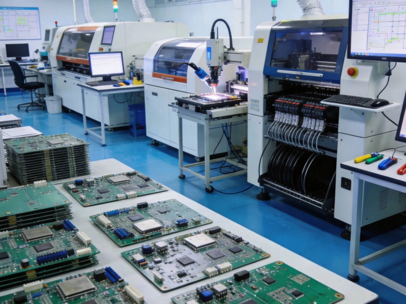
When you workin with High Frequency Pcb Assembly, things get complicated fast. It's not like your regular circuit board job - these boards operates at frequencies that can range from hundreds of megahertz to several gigahertz, and that means every little detail matters. One wrong move with a sensitive component and your whole Signal Integrity goes out the window.
In this article, we gonna dive deep into the real challenges that engineers face during High Frequency Pcb Assembly. We'll talk about what makes these components so sensitive, why standard assembly methods often fail, and what you can actually do to get reliable results. No fluff - just practical insights from someone who's been in the trenches.
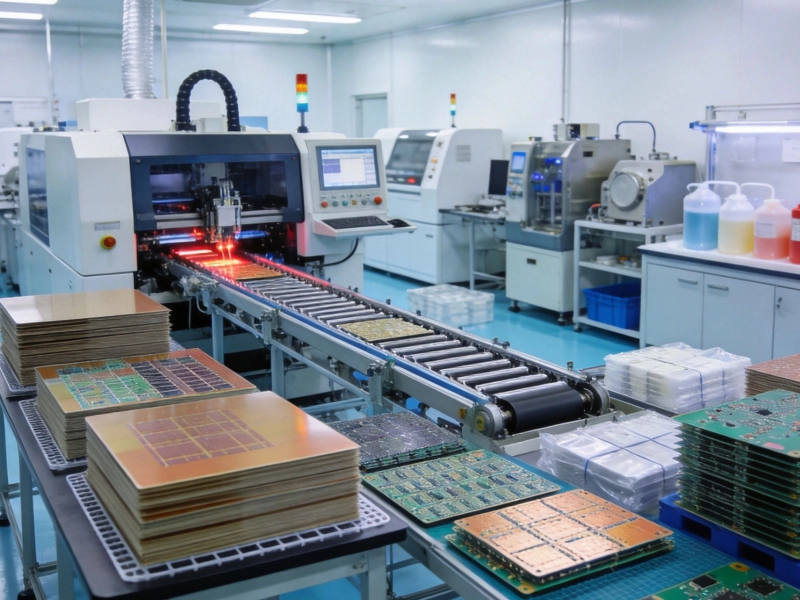
High Frequency Pcb assembly is a specialized field that deals with circuit boards designed to handle RF (radio frequency) and microwave signals. These boards are used in everything from smartphones and WiFi routers to radar systems and Satellite Communications.
What makes High Frequency Pcb assembly different from regular PCB work? Well, it's all about how signals behave at higher frequencies. At low frequencies, you can pretty much treat traces like simple wires. But once you get into the RF range, those traces start acting like transmission lines, and Impedance Matching becomes critical.
Sensitive components in high frequency applications includes things like:
This is probably the biggest headache in high frequency Pcb Assembly. Signal Integrity problems shows up in many ways - reflection, crosstalk, attenuation, and jitter. And most of these issues comes from how components are placed and soldered.
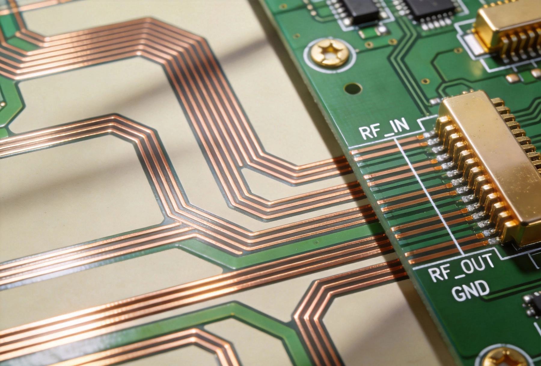
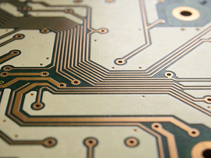
When you dealing with sensitive RF components, even the solder joints themselves can affect signal quality. A solder joint that's slightly too large or irregular can create impedance discontinuities. These discontinuities causes signal reflections that degrade performance.
Common signal integrity problems:
I've seen cases where a board works perfectly in testing but fails in actual use because the assembly process introduced subtle signal integrity problems. It's frustrating because these issues can be really hard to trace back to a specific assembly step.
High frequency components are often more sensitive to heat than regular parts. The assembly process itself involves heating - soldering, reflow, and sometimes even manual touch-up work. This heat exposure can damage sensitive components or affect their calibration.
Some components, like certain RF ICs and crystal oscillators, have strict temperature limits during assembly. Exceeding these limits - even briefly - can permanently change their characteristics. And it's not just the peak temperature that matters; the heating rate and cooling rate can also be critical.
Thermal challenges in assembly:
One thing I learned from experience - always check the component datasheet for assembly temperature requirements. Some manufacturers specify maximum peak temperatures, maximum time above certain temperatures, and even maximum ramp rates. Ignoring these specs is asking for trouble.
In high frequency designs, Component Placement ain't just about getting parts in the right spots - it's about getting them in exactly the right spots with the right orientation. A millimeter of offset or a few degrees of rotation can change how signals propagate through the board.
Antenna components and RF connectors are particularly sensitive to placement accuracy. An antenna element that's slightly off-position can shift the resonant frequency or change the radiation pattern. And RF connectors need precise alignment to maintain impedance continuity.
Placement precision issues:
For really critical placements, some manufacturers use specialized equipment like vision-guided placement systems. These can achieve placement accuracies down to 0.05mm or even better. But that equipment is expensive, and not every assembly house has it.
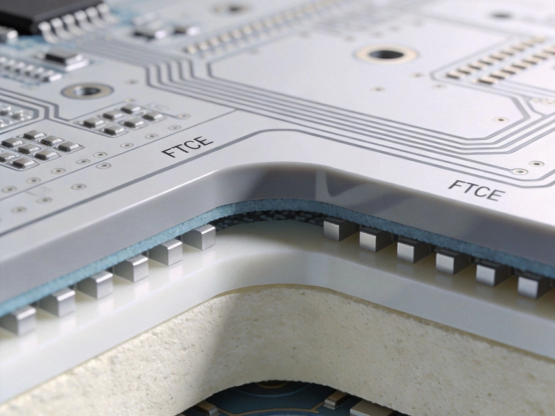
The PCB substrate material matters a lot in high frequency applications. Standard FR-4 works fine for low frequency boards, but at higher frequencies its dielectric losses start becoming significant. You might need to use specialized materials like Rogers, Taconic, or Isola high-frequency laminates.
But material selection introduces assembly challenges too. These high-frequency materials often have different thermal characteristics than FR-4. They might require different soldering temperatures, or they might be more prone to delamination during thermal cycling.
Material-related challenges:
And here's another thing - the materials used for component packaging can also matter. Some RF components use specialized packaging materials that have their own assembly requirements. Mixing incompatible materials can lead to reliability problems over time.
Now that we've looked at the challenges, let's talk about what actually works. These are practical approaches that experienced assembly teams use to get good results with sensitive high frequency components.
High frequency Pcb Assembly needs a controlled environment. This means:
Some high frequency assembly work is done in cleanroom environments, especially for components like MEMS devices. The extra cost of cleanroom assembly can be worth it when you're dealing with extremely sensitive parts.
Standard soldering methods often need modification for sensitive components:
For particularly sensitive components, you might need to solder them after the main reflow process using manual techniques. This adds labor cost but prevents thermal damage.
To maintain signal integrity, everything about component mounting needs to maintain impedance continuity:
This means the PCB design needs to account for assembly realities. The designer and assembly engineer need to work together to make sure the layout supports good assembly practices for sensitive components.
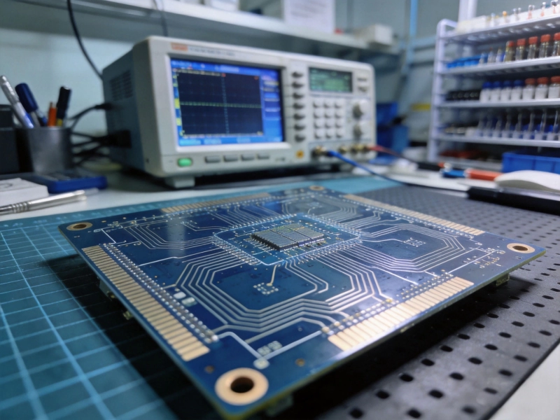
You can't just assume assembly went well - you need to verify signal performance after assembly. This means:
For critical applications, some assembly houses use X-ray inspection to check solder quality under components where visual inspection can't reach. This can catch problems like solder bridging or insufficient solder under RF components.
Not every PCB assembly house has the capability to handle high frequency sensitive components properly. When you're selecting an assembly partner for this type of work, you need to ask the right questions:
A good assembly partner should be able to show examples of similar work they've done and explain their specific processes for handling sensitive components. They should also be willing to work with your design team early in the process to make sure the PCB layout supports their assembly capabilities.
Working with sensitive components in high frequency applications requires careful planning, specialized techniques, and experienced assembly partners. The challenges are real, but with the right approach, you can achieve reliable results.
Need help with your high frequency PCB assembly project? Contact experienced assembly specialists who understand RF requirements and can guide you through the process from design to final testing.
High frequency PCB assembly with sensitive components ain't easy, but understanding the challenges helps you plan better and avoid costly failures. The main issues - signal integrity, thermal management, placement precision, and material compatibility - all interact with each other, so you gotta address them holistically.
Success comes from careful design that accounts for assembly realities, controlled assembly processes that respect component sensitivities, and thorough testing that catches problems early. When all these elements work together, you can build high frequency boards that perform reliably in demanding applications.
The key is recognizing that high frequency assembly is a specialized skill. It's not something you can just throw at a standard assembly line and expect good results. Whether you're designing high frequency boards or assembling them, you need to understand the unique requirements and work with partners who have the right capabilities and experience.
Q: What frequency range requires special PCB Assembly Techniques?
A: Generally, frequencies above 100 MHz start requiring attention to signal integrity during assembly. For frequencies above 1 GHz, specialized techniques become increasingly important. The specific threshold depends on the application requirements.
Q: Can standard FR-4 material be used for high frequency PCBs?
A: FR-4 can work for some high frequency applications up to around 1-2 GHz, but signal losses increase significantly. For frequencies above 2 GHz or applications requiring low loss, specialized high-frequency laminates like Rogers materials are typically needed.
Q: How do I know if a component requires special handling during assembly?
A: Check the component datasheet for assembly requirements. Look for maximum temperature limits, moisture sensitivity levels (MSL), and any notes about vibration or handling precautions. RF components often specify maximum soldering temperatures and durations.
Q: What testing should be done after high frequency PCB assembly?
A: Testing should include RF performance verification (signal integrity, gain, noise figure), impedance measurements at critical points, and visual/X-ray inspection of solder joints. For sensitive components, functional testing that exercises the component in realistic conditions is important.
Q: Why is component placement orientation important in high frequency boards?
A: In high frequency circuits, signal paths act like transmission lines. Component orientation affects how signals enter and exit the component, and can influence impedance matching and signal reflections. Some RF components also have asymmetric internal structures that require specific orientation.
Common Pitfalls to Avoid During Your High Frequency PCB Prototype PhaseJune/18/2026
Why Impedance Control is Critical Even in High Frequency PCB PrototypesJuly/14/2026
Understanding High Frequency PCB Capabilities: Line Width, Spacing, and Layer CountJune/28/2026
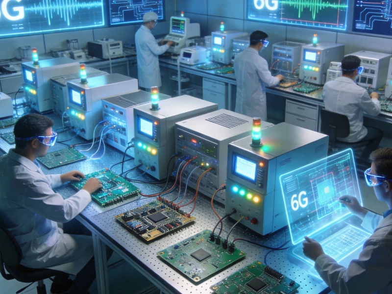
Our Latest High Frequency PCB Capabilities for 6G ResearchMay/29/2026
Advanced High Frequency PCB Fabrication Techniques for Low Loss PerformanceMay/29/2026
Demystifying Impedance Control: Core High Frequency PCB KnowledgeJuly/09/2026
The Ultimate Guide to High Frequency PCB Materials: PTFE, Ceramic, and HydrocarbonJuly/08/2026
The Challenges of High Frequency PCB Assembly: Handling Sensitive ComponentsMay/29/2026