When engineers think about high-frequency PCB design, they typically focus on trace geometry, Dielectric Materials, and impedance calculations. These factors are undeniably important, but there is another variable that quietly influences Signal Integrity at microwave and millimeter-wave frequencies: copper surface roughness. The microscopic hills and valleys on a copper trace surface might be invisible to the naked eye, but they create measurable effects on signal propagation that can make the difference between a design that performs as simulated and one that fails mysteriously in the field.
This guide explores how copper surface roughness affects high-frequency PCB performance, why it matters more as frequencies increase, and what designers and manufacturers can do to control this parameter for reliable RF and microwave applications.
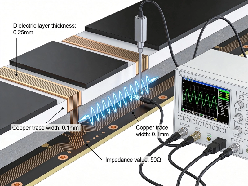
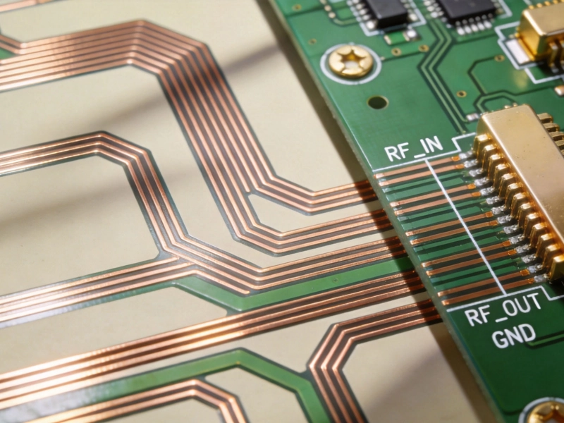
Copper foil used in PCB fabrication is not perfectly smooth. Depending on the manufacturing process and foil type, copper surfaces exhibit roughness ranging from nearly atomically flat for specialty treatments down to several micrometers for standard electrolytic foil. This roughness is typically characterized by two parameters: Ra (arithmetical mean roughness) and Rz (maximum peak-to-valley height). These values, measured in microinches or micrometers, describe the vertical variation on the copper surface.
Standard electrodeposited (ED) copper foil commonly shows Ra values around 0.5-1.5 micrometers. Low-profile (LP) copper reduces this to 0.3-0.5 micrometers. Very low profile (VLP) copper targets 0.2-0.3 micrometers. For the most demanding applications, reverse-treat (RT) foil and specially treated surfaces can achieve Ra values below 0.1 micrometers. The choice of foil type significantly impacts both cost and high-frequency performance.
At high frequencies, current does not distribute uniformly through a conductor. The skin effect causes current to concentrate near the conductor surface, with current density decreasing exponentially from the surface inward. At 10 GHz, the skin depth in copper is approximately 0.65 micrometers. At 30 GHz, it shrinks to about 0.38 micrometers. These values overlap directly with typical copper roughness values, which means the rough surface profile becomes a significant portion of the current-carrying path.
When the skin depth approaches or is smaller than the surface roughness amplitude, the effective current path length increases dramatically. Instead of flowing along a smooth surface, current must navigate around peaks and valleys, following a longer effective path. This longer path translates directly to higher effective resistance and increased conductor loss. The rough surface acts like adding series resistance that is not accounted for in standard trace calculations.
Beyond simple conductor loss, surface roughness affects signal propagation in subtler ways. Rough surfaces cause scattering of electromagnetic waves, which converts some signal energy into unwanted radiation or heat. This scattering effect becomes more pronounced as frequency increases and wavelength approaches the scale of surface features.
The impedance of a transmission line depends on the effective Dielectric Constant and geometry. Surface roughness affects the boundary conditions at the metal-dielectric interface, slightly changing the effective capacitance and inductance of the trace. While this effect is smaller than the conductor loss impact, it can cause discrepancies between simulated and measured impedance that are difficult to diagnose without understanding the roughness contribution.
The relationship between skin depth and frequency explains why roughness becomes increasingly problematic as designs move to higher frequencies. At 1 GHz, skin depth in copper is about 2 micrometers, which is larger than most roughness profiles. The impact on Signal Loss is minimal. At 10 GHz, skin depth drops to 0.65 micrometers, comparable to low-profile copper roughness. At 60 GHz and above, skin depth falls below 0.3 micrometers, smaller than even VLP copper roughness.
This frequency-dependent behavior explains why many designs that worked fine at microwave frequencies failed unexpectedly when extended to millimeter-wave bands. A PCB that showed excellent performance at 5 GHz might exhibit unacceptable loss at 28 GHz, and the culprit is often copper roughness that was acceptable at lower frequencies but becomes limiting at higher frequencies.
For sub-6 GHz 5G applications, standard low-profile copper is usually acceptable. The additional loss from typical roughness profiles adds perhaps 0.1-0.3 dB per inch, manageable with adequate link budget margin. For 28 GHz 5G millimeter-wave links, low-profile copper becomes necessary, with VLP or RT foil preferred for critical paths. At 77 GHz Automotive Radar frequencies, roughness-induced loss becomes a primary design constraint, often requiring the smoothest available copper treatments.
Wi-Fi 6E and emerging Wi-Fi 7 systems operating at 6 GHz face similar challenges. While lower than millimeter-wave frequencies, the 6 GHz band still requires attention to copper roughness for designs targeting maximum range and efficiency. Loss budgets that appeared comfortable at 2.4 GHz may become tight when implemented at 6 GHz if roughness is not controlled.
Several methods exist for measuring copper surface roughness. Optical profilometers use interferometry to map surface topography non-destructively. Mechanical profilometers drag a stylus across the surface to record height variations. Scanning electron microscopy (SEM) provides high-resolution images but requires sample preparation. Atomic force microscopy (AFM) offers the highest resolution but is slow and limited to small sample areas.
For production quality control, optical methods are typically preferred because they are fast, non-contact, and suitable for inline measurement. Mechanical stylus instruments provide more accurate Ra and Rz values but may be too slow for high-volume production inspection. Many PCB manufacturers use statistical sampling with detailed measurement of representative panels to verify roughness consistency across production lots.
Designers should specify copper foil type explicitly in fabrication documentation rather than leaving it to manufacturer defaults. For high-frequency applications, specifying maximum Ra and Rz values ensures consistent material selection. Common specifications for RF PCBs require Ra below 0.5 micrometers for standard applications, below 0.3 micrometers for demanding applications, and below 0.1 micrometers for millimeter-wave designs.
Beyond initial roughness values, specify roughness consistency requirements if critical RF performance must be maintained across a production run. Variation in roughness across a panel or between lots affects yield and performance repeatability. Tighter consistency requirements increase manufacturing cost but ensure more predictable RF performance.
Standard ED copper foil is the most common and least expensive option. The electrodeposition process creates a matte side with moderate roughness and a shiny side that is somewhat smoother. Standard ED copper with Ra values of 0.8-1.5 micrometers on the matte side is generally acceptable for frequencies up to 3-5 GHz but becomes problematic at higher frequencies.
The matte side provides better adhesion to Dielectric Materials due to its rough surface profile. The shiny side offers slightly better high-frequency performance but may delaminate under stress. For many applications, using the shiny side for signal traces and matte side for plane areas provides a reasonable balance between performance and reliability.
Low-profile (LP) copper reduces roughness through modified electrodeposition processes that create a more uniform surface. Ra values typically fall in the 0.3-0.5 micrometer range, making LP copper suitable for applications up to 15-20 GHz. Very low profile (VLP) copper pushes this further to 0.2-0.3 micrometers, extending usable frequencies to 30 GHz and beyond.
The improved surface profile of LP and VLP copper comes at a cost premium, typically 20-50 percent higher than standard ED copper. For high-volume applications where performance matters, this premium is often justified by improved yield and performance margin. For prototypes or low-volume production, the extra cost may be harder to justify unless frequencies truly require it.
Reverse-treated (RT) copper foil flips the traditional profile, with the rough side treated for adhesion while the smooth side provides improved conductivity. This approach delivers the best of both worlds: reliable adhesion and low roughness for signal traces. RT foil can achieve Ra values below 0.1 micrometers on the treated smooth side.
Other specialty treatments include nodular copper that adds microscopic bumps to improve adhesion without significantly increasing roughness, and dendrite-treated surfaces that provide mechanical keying while maintaining smooth electrical surfaces. These treatments offer alternatives when standard foil options do not meet specific performance requirements.
Copper roughness affects several fabrication processes. During etching, rough copper surfaces respond slightly differently than smooth surfaces, potentially affecting trace edge definition. While this effect is typically minor for standard line widths, it becomes more significant for fine-pitch designs where edge smoothness impacts impedance and crosstalk.
Photoresist adhesion may vary with copper surface treatment. The rough matte side of standard ED copper provides excellent mechanical adhesion for photoresist. The smoother shiny side may require surface preparation or different resist formulations to ensure reliable imaging. Manufacturers develop optimized processes for each foil type to maintain consistent quality.
Surface roughness influences how copper bonds to prepreg and dielectric materials during lamination. Rougher surfaces provide more surface area for mechanical bonding, which generally improves adhesion and reduces delamination risk. However, if the dielectric material does not flow properly into the surface profile, voids can form that create reliability issues.
Low-profile and VLP copper may require modified bonding processes or alternative prepreg formulations to achieve reliable adhesion. Some manufacturers use thin tie layers or specialty adhesives designed specifically for smooth copper surfaces. These additions increase cost and may affect electrical properties, requiring careful evaluation.
Many PCB finishes interact differently with rough versus smooth copper surfaces. Electroless nickel immersion gold (ENIG) plating follows the underlying copper profile, so rough copper results in rough nickel surfaces that affect high-frequency performance. This is particularly problematic because ENIG is a common finish for RF applications due to its excellent solderability and shelf life.
Alternative finishes like immersion silver or OSP (organic solderability preservative) may track underlying roughness less severely. For the smoothest possible surface finish, special post-plating polishing orbuffing processes can reduce roughness after plating but add significant cost and require careful process control.
Start by selecting materials specifically designed for high-frequency applications. Many high-frequency laminate manufacturers offer low-roughness copper options as part of their product families. These matched material systems ensure compatibility between dielectric properties and copper profile, simplifying specification and reducing risk.
When specifying materials, request the actual roughness values rather than accepting generic descriptions like low-profile. Different manufacturers define low-profile differently, and the actual Ra values can vary significantly. Requesting specific measurement data or limiting purchasing to materials with certified roughness values ensures consistency.
Stack-up design can mitigate some roughness effects. Using thinner dielectrics between signal layers and reference planes increases capacitance per unit length, which reduces the relative impact of roughness-induced inductance variation. This approach trades off routing density and manufacturing complexity against roughness sensitivity.
Route critical high-frequency signals on layers with the smoothest copper available. Reserve rougher layers for lower-frequency signals, power distribution, and ground planes where roughness impact is less critical. This layered approach optimizes cost versus performance by reserving premium materials for the signals that need them most.
Accurate high-frequency simulation must include roughness models. Most RF simulation tools include roughness correction factors or models that can be parameterized based on measured roughness values. Using these models with realistic roughness inputs produces simulations that better match measured performance.
Calibrate simulation models against test boards fabricated with the same materials and processes planned for production. By measuring actual performance and correlating with simulations, you can develop roughness parameters that produce accurate predictions. This calibration process is especially valuable for demanding applications where performance margin is tight.
Establish incoming inspection protocols that verify copper roughness for critical applications. Rather than relying solely on manufacturer certifications, spot-check incoming materials with optical profilometry or other measurement methods. This verification catches material substitutions or process variations that could affect performance.
Documentation of incoming inspection results builds a material history that supports failure analysis if problems arise. When materials from different lots show different roughness values, this data helps explain performance variations and supports warranty claims with suppliers.
Monitor fabrication processes that might affect surface roughness. Plating processes, cleaning steps, and handling procedures can all influence final surface profile. Maintaining consistent process parameters ensures that roughness remains within specified limits across production runs.
Statistical process control applied to roughness measurements helps identify trends before they cause quality problems. If roughness values drift upward over time, this signals a need for process adjustment before out-of-spec material reaches production. Preventive control is far more cost-effective than sorting or rejecting finished boards.
Smoother copper costs more, but the premium varies significantly by foil type and volume. Standard ED copper is the baseline. LP copper typically adds 15-30 percent to material cost. VLP copper adds 30-50 percent. RT and specialty foils can cost 2-3 times standard copper. These premiums compound with overall board cost, so the absolute dollar impact depends on the specific application.
Evaluate whether the performance benefit justifies the cost premium for your specific application. If your design has significant margin at the frequency of interest, standard copper might perform adequately with lower cost. If you are pushing performance limits with tight loss budgets, investing in smoother copper may be necessary for reliable production.
Consider total cost beyond raw material cost. Smoother copper may enable simpler designs with shorter signal paths or less amplification, partially offsetting material premiums. Better yield from more predictable performance can reduce rework and scrap costs. Field failures from roughness-related performance issues carry costs far beyond the material premium.
For high-volume applications where performance consistency matters, investing in tighter roughness control pays dividends across production runs. The improved predictability reduces yield loss and warranty returns, making premium materials economically attractive even when they appear expensive in isolation.
Research continues into copper deposition and treatment methods that produce even smoother surfaces at lower cost. Advanced electrodeposition processes, alloy additions, and post-deposition treatments show promise for improving surface quality without the expense of current specialty foils. Some manufacturers are developing foil products specifically targeting millimeter-wave applications.
Alternative conductor materials, including silver inks and graphene coatings, offer potential advantages for high-frequency applications. While these technologies remain largely experimental, they may eventually supplement or replace traditional copper for the most demanding applications where surface quality is paramount.
As advanced packaging technologies like embedded components and fan-out wafer-level packaging gain adoption, surface roughness considerations extend beyond traditional PCB substrates. These emerging technologies introduce new surface interfaces and materials that require careful characterization for high-frequency performance.
Understanding roughness effects will become increasingly important as systems combine multiple packaging technologies. The boundary between IC packaging and PCB continues blurring, and surface effects that were negligible at board level may become significant at the chip-package interface.
Surface roughness is an often-overlooked factor in high-frequency PCB design that becomes increasingly critical as frequencies climb toward microwave and millimeter-wave bands. The skin effect causes current to concentrate in the rough surface layer, directly converting surface topography into additional conductor loss. Beyond simple loss, roughness affects impedance, causes scattering, and creates discrepancies between simulated and measured performance.
Managing surface roughness requires attention throughout the design and manufacturing process. Material selection must explicitly address foil type and roughness specifications. Stack-up design should route critical signals on smoothest-available layers. Manufacturing must implement quality control measures that verify roughness consistency. The cost premiums for smoother copper are often justified by improved performance and yield, particularly for demanding applications where margin is tight.
As 5G networks expand into millimeter-wave bands and emerging applications push to even higher frequencies, surface roughness control will become increasingly important for PCB designers and manufacturers. Building expertise in this area now positions you to handle the higher-frequency challenges ahead.
At high frequencies, current concentrates near the conductor surface due to the skin effect. When skin depth approaches the scale of surface roughness, current must follow the rough profile, increasing effective path length and resistance. This adds conductor loss that is not predicted by ideal trace calculations. Roughness also affects impedance through boundary condition changes and causes scattering of electromagnetic energy.
For 28 GHz and higher frequencies, Ra values below 0.3 micrometers are typically necessary, with Ra below 0.1 micrometers preferred for the most critical paths. Very low profile (VLP) or reverse-treated (RT) copper foil provides the required smoothness. Standard or even standard low-profile copper usually introduces unacceptable loss at these frequencies.
ENIG (Electroless Nickel Immersion Gold) follows the underlying copper profile, so rough copper results in rough nickel surfaces. For frequencies below 10 GHz, this effect is usually manageable. For millimeter-wave applications, consider alternative finishes like immersion silver or specify post-plating polishing to reduce effective roughness.
Specify maximum Ra and Rz values explicitly in fabrication documentation. For RF applications, require Ra below 0.5 micrometers as a baseline, with lower values for more demanding applications. Request certified test reports or perform incoming inspection to verify roughness meets specifications.
No, the impact increases dramatically with frequency because skin depth decreases. At frequencies where skin depth is much larger than roughness amplitude, the effect is negligible. As skin depth approaches roughness values, impact becomes significant. Above 10 GHz, roughness control becomes increasingly critical for reliable performance.
Need help with high-frequency PCB design and surface roughness requirements? Our engineering team has extensive experience with RF and millimeter-wave PCB fabrication. Contact us to discuss your specific frequency requirements and learn how we can help optimize your design for reliable high-frequency performance.
High Frequency PCB Fabrication: Managing Dielectric Constant (Dk) TolerancesJune/09/2026
Advanced High Frequency PCB Fabrication Techniques for Low Loss PerformanceMay/29/2026
High Frequency PCB Assembly Best Practices for 5G and RF ModulesJune/08/2026
The Benefits of Rapid High Frequency PCB PrototypingMay/29/2026
Handling Sensitive ComponentsMay/29/2026
7 Key Factors to Consider When Choosing a High Frequency PCB ManufacturerMay/29/2026
Quality and Cost Analysis of High-Frequency Printed Circuit Board Manufacturers in China and the WestJune/04/2026
The Challenges of High Frequency PCB Assembly: Handling Sensitive ComponentsMay/29/2026