Open Nav
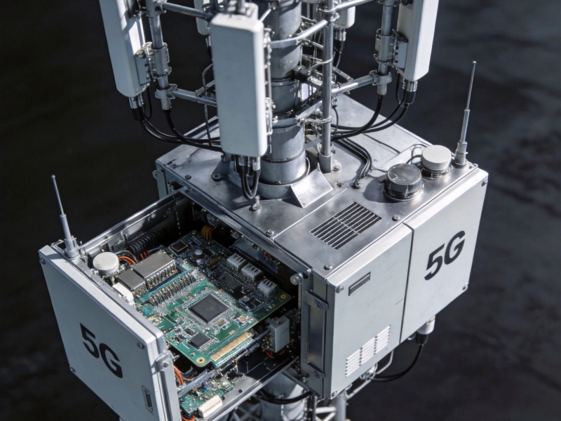
The global rollout of 5G networks represents the most significant advancement in telecommunications technology since the transition from analog to digital. But 5G isn't just faster smartphones—it demands a complete reimagining of network infrastructure, from massive antenna arrays to tiny embedded modules. At the heart of this transformation lies High Frequency Pcb technology that enables the signal processing, power amplification, and antenna systems making next-generation connectivity possible.
Unlike conventional PCBs serving low-frequency applications, high frequency PCBs must maintain Signal Integrity at frequencies where traditional materials introduce unacceptable losses. From Sub-6GHz deployments to millimeter-wave systems operating above 24GHz, the telecommunications industry pushes PCB technology to its limits and beyond. Understanding these applications helps engineers, product managers, and technology decision-makers appreciate how advanced materials science enables the connected world we increasingly depend on.
As someone who's worked closely with telecommunications equipment manufacturers and PCB suppliers over the past decade, I've witnessed firsthand how High Frequency Pcb technology has evolved from a specialized niche to an essential capability for any company participating in the 5G ecosystem. This article explores the top applications driving demand for high frequency PCBs and the technical requirements that make these boards so challenging to manufacture.
A PCB enters the "high frequency" category when operating frequencies exceed approximately 1GHz, though the term is most commonly applied to RF and microwave circuits operating from 5GHz to 100GHz and beyond. At these frequencies, conventional FR-4 materials introduce several problems that high frequency PCBs must address:
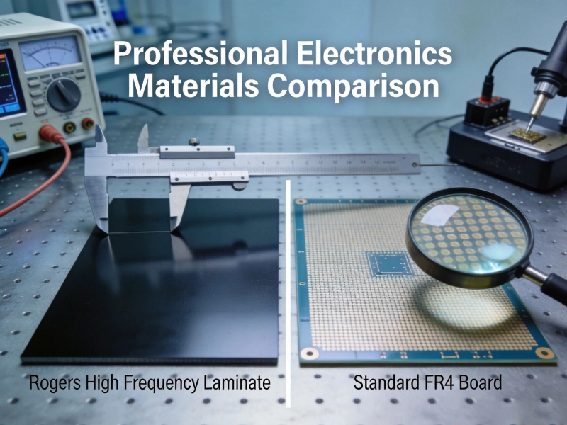
The distinguishing characteristic of High Frequency Pcb Materials is their Dielectric Constant (Dk) and dissipation factor (Df). Lower, more stable values indicate better high frequency performance.
High frequency PCBs utilize specialized substrate materials:
Material selection balances electrical performance against cost, manufacturability, and mechanical requirements. Not every application needs the absolute lowest loss—often a moderate-loss material at lower cost meets requirements adequately.
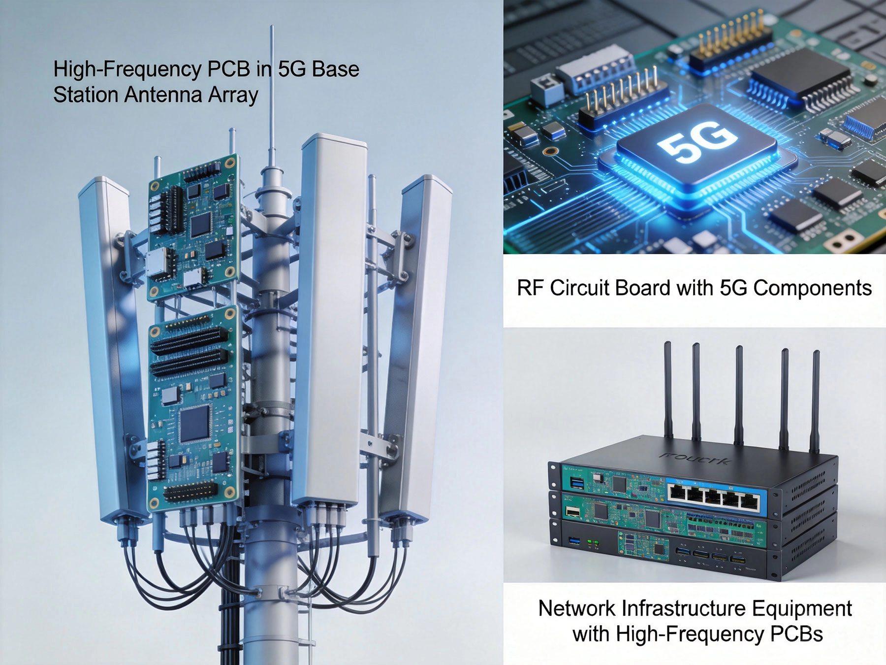
5G base stations employ Massive MIMO (Multiple Input, Multiple Output) technology using antenna arrays with 64, 128, or even 256 individual antenna elements. This massive number of elements enables spatial multiplexing that dramatically increases network capacity and efficiency. But Massive MIMO places extraordinary demands on PCB technology:
High frequency PCBs form the backbone of these antenna systems, providing the low-loss transmission lines and precise Impedance Control that enables efficient power distribution across the array. Without advanced Pcb Materials, Massive MIMO systems would be impractical due to excessive losses and phase errors.
Beamforming networks distribute RF signals to antenna elements with appropriate phase and amplitude. These networks typically use:
High frequency PCBs enable these networks to operate with minimal loss and consistent phase relationships across the frequency band. The precise material properties of PTFE-based boards ensure predictable performance across temperature variations and manufacturing runs.
Modern antenna systems integrate active electronics directly behind the antenna elements:
These active assemblies often use multi-layer high frequency PCBs combining RF and digital functionality in unified assemblies that minimize interconnect losses between stages.
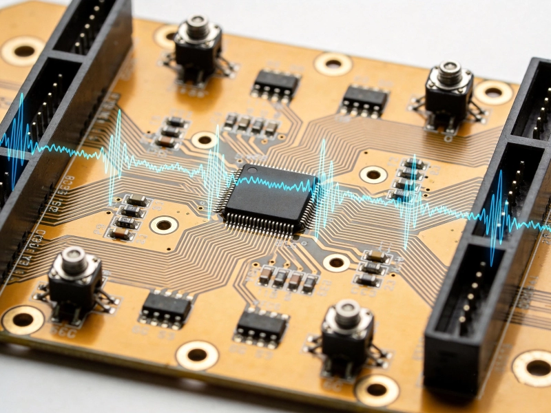
5G devices—from smartphones to IoT sensors—pack sophisticated RF front-ends into increasingly small form factors. The RF front-end module (FEM) handles transmit amplification, receive filtering, and antenna switching, all within a footprint measured in millimeters. High frequency PCBs make this miniaturization possible through:
Modern smartphone RF front-ends contain dozens of components—switches, filters, amplifiers, and matching networks—integrated into compact modules using advanced high frequency PCB technology.
5G devices require sophisticated filtering to isolate signals in crowded spectrum:
High frequency PCBs provide the substrate for planar filters and also interface with discrete filter components through controlled-impedance connections that maintain Signal Integrity.
Modern RF front-ends use sophisticated switching to connect antennas to different radio chains:
These switches require low-loss, high-linearity PCBs that minimize signal degradation while handling significant power levels during transmission.
True 5G performance requires millimeter-wave spectrum (above 24GHz) where massive bandwidth enables multi-gigabit data rates. However, mmWave presents unique challenges:
High frequency PCBs become even more critical at mmWave frequencies where losses compound rapidly. Even small imperfections in material properties or manufacturing cause significant signal degradation.
5G networks require high-capacity backhaul links connecting base stations to the core network. Point-to-point microwave radio systems operating at 60GHz, 70GHz, and 80GHz provide fiber-like capacity without fiber deployment. These systems use high frequency PCBs for:
The demanding environment—often outdoor installations with wide temperature ranges—requires PCBs that maintain stable electrical properties under thermal stress.
Fixed wireless access (FWA) delivers broadband to homes and businesses using 5G mmWave signals. Customer premises equipment (CPE) includes:
High frequency PCBs in CPE must balance cost, performance, and reliability for consumer-grade products deployed in diverse environments.
While 5G is wireless, the backhaul network often uses optical fiber. But the interfaces between wireless and wireline systems require high frequency PCBs:
These systems often operate at 10Gbps, 25Gbps, and 100Gbps per lane, requiring PCB materials and design techniques approaching pure microwave frequencies.
Data centers and central offices contain network switches routing millions of connections:
While not strictly "RF" applications, these boards use many of the same high-speed design techniques and sometimes specialized high-frequency materials for optimal signal integrity.
Microwave radio remains important for backhaul in areas without fiber access:
Microwave radio operating from 6GHz to 42GHz uses high frequency PCBs throughout for signal processing, frequency conversion, and power amplification.
Low Earth orbit (LEO) satellite constellations are transforming global connectivity. These systems require sophisticated electronics for:
High frequency PCBs for space applications face unique requirements:
Space-qualified high frequency PCBs undergo rigorous testing and screening to ensure reliable operation in the harsh space environment.
Modern satellite terminals use electronically steered phased arrays:
These systems operate at Ka-band (20-30GHz) and V-band (40-75GHz), requiring ultra-low-loss PCBs and sophisticated thermal management.
Connected vehicles rely on high frequency electronics for multiple functions:
Automotive applications demand exceptional reliability, operating in harsh thermal environments while meeting stringent safety requirements.
Automotive radar systems operating at 77GHz and 79GHz provide:
These systems require ultra-high-frequency PCBs with exceptional loss characteristics. Rogers RO3003 and similar materials provide the performance needed for millimeter-wave radar at automotive price points.
Modern radar modules integrate antennas directly into the PCB or package:
This integration reduces cost and size while improving reliability compared to separate antenna modules.
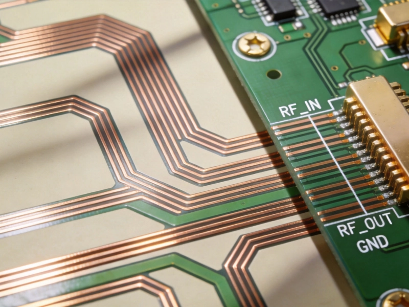
High frequency PCBs must meet demanding electrical specifications:
Beyond electrical performance, high frequency PCBs face mechanical challenges:
High frequency Pcb Manufacturing requires specialized capabilities:
Not all PCB manufacturers can produce high frequency boards reliably. Working with experienced suppliers is essential for consistent quality.
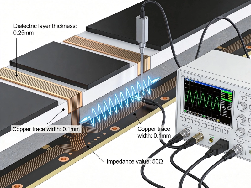
Maintaining consistent transmission line impedance is critical:
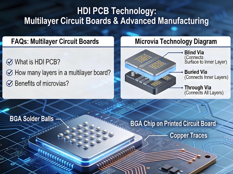
Vias introduce discontinuities that degrade high-frequency performance:
Careful via design—back-drilling, blind/buried vias, and via-in-pad techniques—minimizes these effects.
Proper grounding ensures consistent performance:
High frequency materials cost significantly more than standard FR-4:
Material selection balances performance against cost for each application.
High frequency Pcb Manufacturing requires more careful processing:
Balance performance against cost:
Research is already progressing toward 6G systems operating at sub-terahertz frequencies (90GHz-300GHz):
Artificial intelligence is transforming network operations:
These systems require high-performance computing that also benefits from advanced PCB technology.
Optical and electronic integration continues advancing:
High frequency PCB technology forms the invisible foundation of modern telecommunications infrastructure. From 5G base station antenna arrays to satellite communication terminals, from automotive radar systems to network infrastructure equipment, the demanding requirements of high-frequency operation push PCB technology to its limits.
The applications explored in this article represent billions of dollars in equipment deployed globally—each board a carefully engineered solution balancing electrical performance, mechanical reliability, and cost effectiveness. Understanding these applications helps appreciate the engineering sophistication behind the devices we often take for granted.
As telecommunications technology continues advancing toward 6G and beyond, high frequency PCB requirements will only increase. New materials, manufacturing techniques, and design methodologies will emerge to meet these challenges. The engineers and manufacturers who master these technologies will enable the next generation of connectivity that transforms how we live, work, and communicate.
For companies developing products in the telecommunications space, partnering with experienced high frequency PCB manufacturers is essential. The specialized knowledge required for these boards can't be substituted with generic manufacturing capabilities. Invest time in understanding your material and design requirements, work closely with your PCB supplier, and verify performance through comprehensive testing.
The connected future depends on high frequency technology. Make sure your designs meet the challenge.
High frequency PCBs typically operate at frequencies above 1GHz, with the term most commonly applied to RF and microwave circuits from 5GHz to 100GHz and beyond. These boards use specialized low-loss materials (like PTFE or ceramic-filled hydrocarbons) rather than standard FR-4 to minimize Signal Loss and maintain consistent impedance at high frequencies.
FR-4 materials have significantly higher dielectric loss at high frequencies, causing signal attenuation that makes them unsuitable for 5G applications. At frequencies above 5GHz, FR-4 losses become prohibitive. High Frequency Pcb Materials like Rogers RO4003 or RT/duroid provide much lower dissipation factors, maintaining signal integrity across the frequency range required for 5G operation.
The most common high frequency materials include Rogers RT/duroid (PTFE-based), Rogers RO4000 series (ceramic-filled hydrocarbon), Taconic TLC and RF series, and Arlon materials. Selection depends on frequency range, cost constraints, and mechanical requirements. PTFE materials offer the best electrical performance but are more expensive and challenging to manufacture.
High frequency PCBs differ in material (low-loss dielectrics vs. standard FR-4), design rules (tighter tolerances, Controlled Impedance), manufacturing processes (specialized handling for PTFE, tighter process control), and testing (impedance verification, high-frequency electrical testing). These differences increase cost but enable reliable operation at frequencies where standard materials fail.
6G systems will push to even higher frequencies (sub-terahertz and terahertz ranges), requiring new materials with even lower losses, advanced manufacturing techniques for finer features, and integration technologies combining multiple functions. Research is already exploring engineered metamaterials, ultra-low-loss substrates, and novel packaging approaches for next-generation systems.
High frequency PCB materials cost 5-20x more than FR-4 depending on the specific material. Manufacturing costs are also higher due to more complex processing requirements and lower yields. Overall, high frequency PCBs typically cost 3-10x more than equivalent standard PCBs. However, for 5G and telecommunications applications, the performance benefits justify the cost premium.
High frequency PCBs require comprehensive testing including impedance verification (time-domain reflectometry), insertion loss measurement, dielectric constant verification, thermal testing for temperature stability, and high-frequency electrical testing across the operating frequency range. X-ray inspection of plated through-holes and microsection analysis verify manufacturing quality.
Yes, high frequency PCBs are manufactured in high volumes for consumer applications like smartphones and automotive radar. Volume production improves yields and reduces per-unit costs significantly. However, volume production requires careful process control and quality systems to maintain consistency across millions of boards.
High Frequency PCB Fabrication: Managing Dielectric Constant (Dk) TolerancesJune/09/2026
The Benefits of Rapid High Frequency PCB PrototypingMay/29/2026
Handling Sensitive ComponentsMay/29/2026
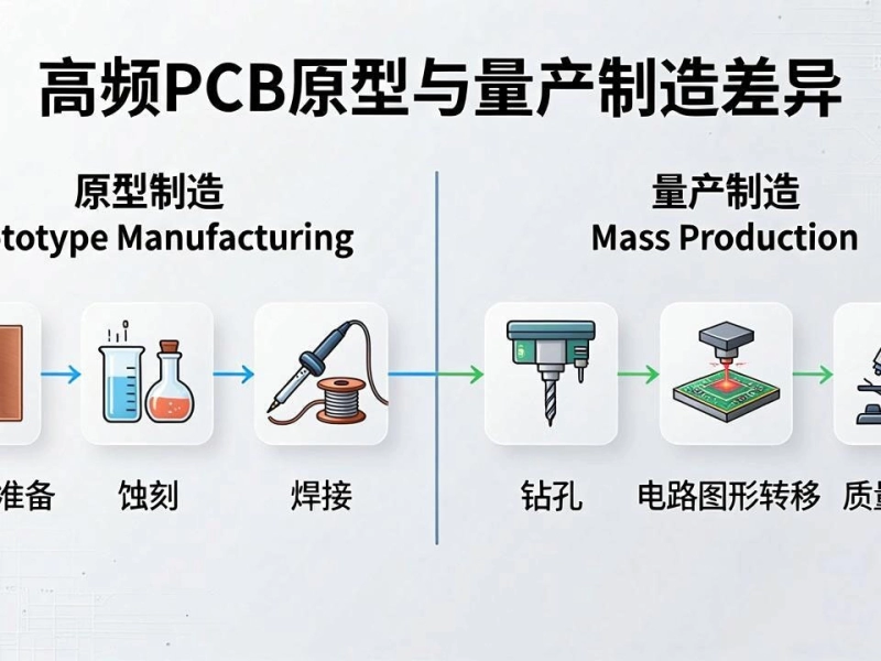
High Frequency PCB Prototype vs. Mass Production: Key Differences in FabricationJune/05/2026
Pushing the Limits: Our Latest High Frequency PCB Capabilities for 6G ResearchJune/11/2026
Essential High Frequency PCB Knowledge for Hardware Engineers and DesignersMay/29/2026
Top High Frequency PCB Applications in the 5G and Telecommunications IndustryMay/29/2026
Choosing the Right High Frequency PCB MaterialsMay/29/2026