Open Nav

High frequency printed circuit boards operate under rules that differ fundamentally from those governing low-speed digital designs. At frequencies above approximately 1 GHz, trace dimensions become comparable to signal wavelengths, transforming PCB traces from simple electrical connections into Transmission Lines governed by electromagnetic wave principles. Engineers entering high frequency design must understand these principles to create boards that perform reliably at RF and microwave frequencies.
This guide provides the foundational knowledge engineers need for High Frequency Pcb design, focusing particularly on stack-up design which forms the structural foundation for successful RF implementations. Whether you are designing for 5G communications, radar systems, automotive sensors, or high-speed data links, the principles covered here apply across the spectrum of high frequency applications.
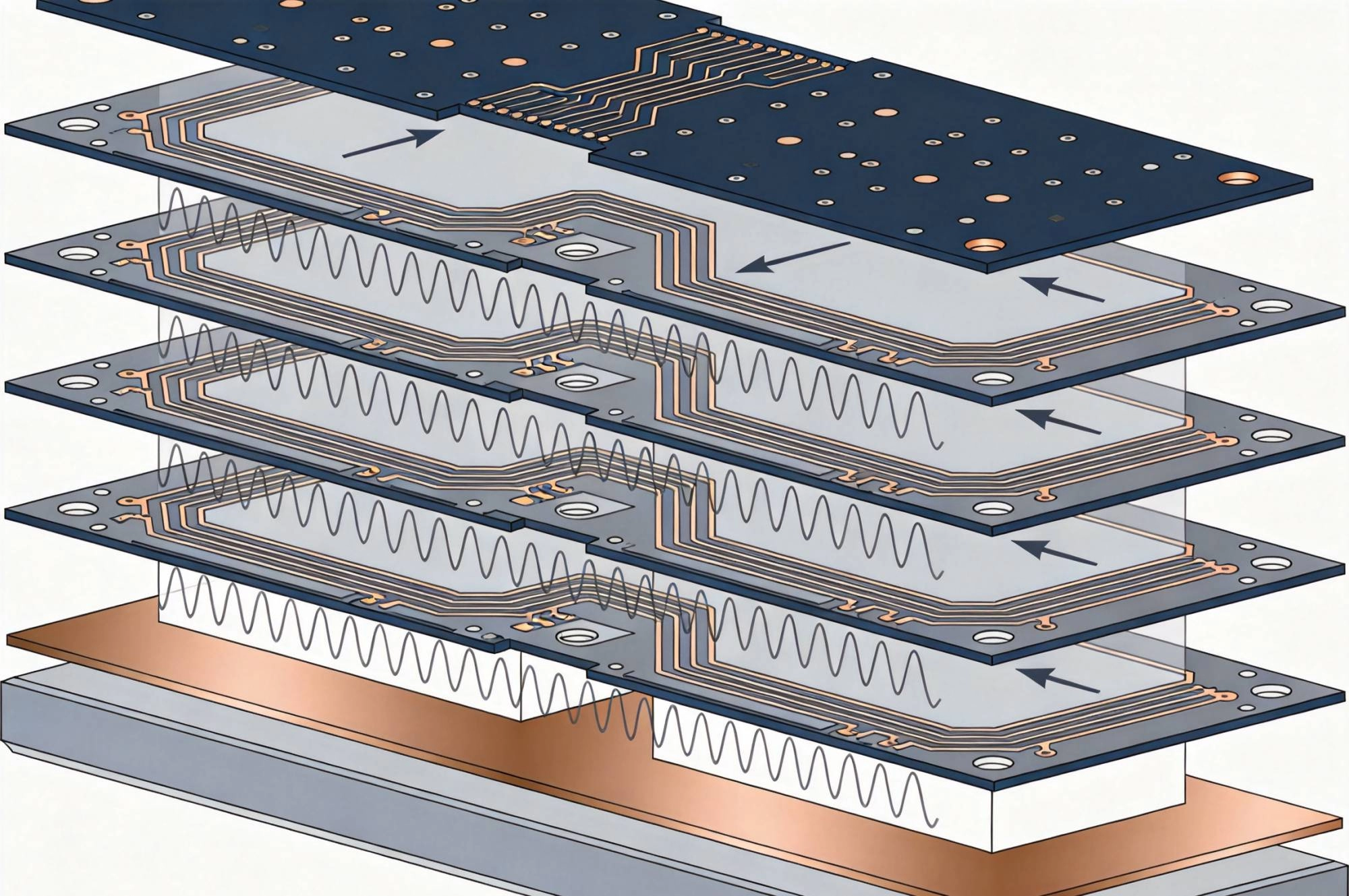
At low frequencies, PCB traces behave as simple resistive conductors. Current flows uniformly through the cross-section, and circuit behavior follows familiar lumped-element models. This simplicity breaks down as frequency increases and signal wavelengths become comparable to trace dimensions. Engineers must then account for distributed parameter effects including capacitance between parallel traces, inductance along trace length, and propagation delay through the medium.
The transition frequency where transmission line effects become significant depends on both trace geometry and signal rise time. For digital signals with nanosecond rise times, effects become noticeable at frequencies above 100 MHz. For analog RF applications, transmission line design matters even at lower frequencies where wavelengths remain relatively long.
Signals in PCBs propagate as electromagnetic waves through the dielectric material surrounding conductors. The propagation velocity depends on the Dielectric Constant of the material, with signals traveling slower in materials with higher dielectric constants. This velocity reduction affects wavelength, impedance calculations, and timing relationships in high speed designs.
The relationship between Dielectric Constant and propagation velocity means that materials with consistent dielectric properties produce more predictable high frequency behavior. Variations in dielectric constant across a board or between manufacturing batches introduce uncertainties that degrade performance in sensitive applications. Material specification and vendor qualification therefore matter more in high frequency designs than in digital applications.
At high frequencies, current does not distribute uniformly through conductor cross-sections. Instead, current concentrates near conductor surfaces, a phenomenon called Skin Effect. The skin depth, or distance from the surface where current density falls to 1/e of its surface value, decreases as frequency increases. At 10 GHz, skin depth in copper is approximately 0.6 micrometers, meaning essentially all current flows within the outermost micron of the conductor.
Skin Effect has several important implications for High Frequency Pcb design. Surface roughness affects impedance because current must follow the roughened surface path, effectively increasing resistance. Plating quality matters because current flows primarily in surface layers. And trace width tolerances become more critical because the conducting cross-section changes more rapidly with width variations at high frequencies.
Transmission line theory provides the framework for understanding and designing high frequency PCB interconnects. The key parameters—Characteristic Impedance, propagation constant, and reflection coefficient—determine how signals behave as they travel through PCB traces. Engineers must control these parameters to ensure signals reach their destinations without distortion or excessive loss.
Characteristic Impedance represents the ratio of voltage to current for a wave propagating along a uniform transmission line. For PCB traces, typical target impedances include 50 ohms for single-ended signals and 100 ohms for differential pairs. Maintaining consistent impedance throughout an interconnect eliminates reflections that degrade signal quality.
Microstrip traces run on the surface of a PCB with dielectric material below and air above. This common configuration offers easier manufacturing and component access but provides less consistent Impedance Control due to variability in the dielectric constant of the air above the trace. Microstrip impedance depends on trace width, dielectric thickness, and copper weight.
Stripline traces run between two ground planes with dielectric material above and below. This buried configuration provides consistent dielectric environment and excellent shielding from external interference. Stripline impedance depends on trace width, dielectric thickness to each plane, and the dielectric constant of the laminates. The additional manufacturing complexity and higher cost of stripline often pay dividends in improved Signal Integrity.
Impedance calculations for PCB Transmission Lines require solving electromagnetic field equations that relate geometry to electrical parameters. For practical design work, engineers use calculation tools or reference tables that provide impedance values for standard configurations. These tools accept trace width, dielectric thickness, and material properties as inputs, producing impedance and other parameters as outputs.
Popular calculation tools include free online calculators for quick estimates, standalone software packages for detailed analysis, and field solver tools that solve Maxwell's equations numerically for complex geometries. Field solvers provide the highest accuracy and can handle non-standard geometries that reference tables cannot address. However, field solver setup requires more expertise and computation time than simpler approaches.
PCB stack-up design determines the layer structure, material selection, and thickness allocation that form the physical foundation for high frequency performance. A well-designed stack-up enables Controlled Impedance traces, provides adequate ground referencing, and supports components requiring buried or blind vias. Stack-up decisions made early in design become expensive to change later, making careful planning essential.
Stack-up design balances competing requirements including Impedance Control, routing density, manufacturing feasibility, and cost. Designers must also accommodate mechanical requirements, thermal management needs, and specific constraints imposed by components or applications. The resulting stack-up reflects these diverse considerations in a manufacturable configuration.
Effective high frequency stack-ups place signal layers adjacent to solid ground planes. This configuration provides consistent impedance referencing and minimizes radiated emissions by containing electromagnetic fields between signal and ground layers. The best practice places signal traces on outer layers referenced to adjacent inner ground planes, keeping high frequency currents close to ground references.
Ground plane continuity matters as much as presence. Slots, splits, or other discontinuities in ground planes disrupt return current paths and create impedance variations. High frequency stack-up design should minimize plane discontinuities and route signal traces only over continuous ground references. When plane splits are unavoidable, careful analysis ensures that Signal Integrity effects remain within acceptable bounds.
Layer thickness allocation determines trace-to-reference distances that control impedance. Thinner dielectrics support narrower traces for a given impedance, enabling higher routing density. However, thinner dielectrics may not provide adequate voltage isolation between layers and can create manufacturing challenges for thick copper or heavy components.
Dielectric material selection affects impedance consistency, loss characteristics, and cost. Standard Fr-4 works adequately for many high frequency applications up to several GHz. Beyond that range, specialized high-frequency laminates with lower loss tangents and more consistent dielectric properties become necessary. Material selection should match application frequency range and loss requirements.
Controlled Impedance traces maintain consistent characteristic impedance throughout their length, preventing reflections that degrade signal quality. Achieving controlled impedance requires precise control of trace geometry, dielectric properties, and manufacturing tolerances. The tolerance budget must account for variations in all contributing factors across production boards.
Typical impedance tolerances for high frequency applications range from ±5% to ±10%, with tighter tolerances required for more sensitive applications. Achieving tight tolerances may require special manufacturing processes, enhanced inspection, or selection of specific impedance values that are more controllable with available materials and processes.
Trace width variations directly affect impedance. The sensitivity depends on the impedance value and geometry, but typical sensitivity ranges from 1 to 2 ohms per mil of width variation. A ±0.5 mil width tolerance therefore produces ±1 ohm impedance variation, which may be acceptable for some applications but problematic for others.
Etching process variations dominate trace width tolerances in Pcb Manufacturing. Standard processes typically achieve ±0.5 mil minimum feature tolerance, though this varies by manufacturer and board complexity. Designers specifying very fine traces or very tight impedance tolerances should verify manufacturer capabilities before finalizing designs.
Dielectric constant variations in laminate materials affect impedance because impedance depends on the square root of dielectric constant. Material suppliers specify typical dielectric constant values, but actual values vary with resin content, glass weave distribution, and manufacturing process parameters. The variation tolerance typically ranges from ±2% to ±5% depending on material type and manufacturer.
Dielectric constant variation can result from non-uniform resin distribution in glass-reinforced laminates. Glass weave fibers have different dielectric constants than resin, so areas with more glass under a trace see different effective dielectric constants than areas with more resin. This effect, called weave micro-loading, can cause impedance variations along trace length that prove problematic for sensitive applications.
Material selection profoundly impacts high frequency PCB performance. The dielectric constant, loss tangent, thermal stability, and mechanical properties of laminate materials all influence achievable performance. Material costs range widely, with high-performance materials commanding significant premiums over standard Fr-4. Understanding material characteristics guides selection that balances performance and cost appropriately.
High Frequency Laminate materials fall into several categories distinguished by their composition and properties. Each category offers different trade-offs between electrical performance, thermal capability, moisture resistance, and cost. Selection should consider all relevant requirements rather than optimizing any single parameter.
Standard FR-4 epoxy-glass laminates remain the workhorse of the PCB industry due to their excellent cost-to-performance ratio for general applications. Modern FR-4 materials have improved high frequency characteristics compared to older formulations, making them suitable for applications up to approximately 10 GHz with careful design. Loss tangent values in the 0.02 range cause acceptable Insertion Loss for many applications.
The primary advantages of FR-4 include broad availability, established manufacturing processes, competitive pricing, and extensive design experience across the industry. The primary disadvantages include dielectric constant variation with temperature and frequency, higher loss than specialized materials, and limited thermal capability for lead-free assembly or high-temperature operation.
High-speed laminates offer improved electrical properties including lower loss tangent, more consistent dielectric constant, and better thermal stability. These materials use modified epoxy systems, hydrocarbon ceramic fillers, or PTFE (Teflon) substrates to achieve performance improvements. Selection among these materials depends on specific performance requirements and cost constraints.
PTFE-based materials offer the best electrical performance, with loss tangents below 0.002 and excellent high frequency characteristics. However, PTFE materials present manufacturing challenges including CTE mismatch with copper, difficulty with through-hole plating, and higher costs. These materials suit applications where electrical performance justifies the additional manufacturing complexity and cost.
Many high frequency designs use hybrid stack-ups combining different materials to optimize cost and performance. A common approach places high-frequency materials only in layers requiring critical electrical performance while using standard materials elsewhere. This hybrid approach reduces material costs while meeting performance requirements where they matter most.
Hybrid stack-ups require attention to material compatibility during lamination. Different materials have different thermal expansion characteristics, cure temperatures, and pressure requirements that may conflict during multilayer bonding. Manufacturers experienced with hybrid constructions can advise on compatible material combinations and appropriate processing parameters.
Differential signaling transmits data using paired traces with equal and opposite voltages. This technique provides common-mode noise rejection, reduces radiated emissions, and doubles the effective signal swing. Differential pairs are ubiquitous in high speed digital standards including USB, PCIe, HDMI, and Ethernet, making differential design knowledge essential for modern high frequency PCB engineers.
Effective differential design maintains tight coupling between pair members, controls differential impedance to specification, and ensures symmetric trace lengths. Violations of these principles degrade the benefits of differential signaling and may cause signal integrity problems that affect system performance.
Differential pairs can be routed with tight coupling, where pair members run close together, or decoupled, where they run with larger spacing. Tight coupling provides better common-mode noise rejection and reduces electromagnetic coupling to adjacent traces. Decoupling provides easier manufacturing tolerances and more routing flexibility.
Traditional digital design guidance favored decoupled routing because trace width dominated impedance calculation, and coupling contributed only small variations. Modern high-speed serial links, however, often specify coupled routing for improved signal integrity. Follow interface specifications when present, and understand the trade-offs when designing interfaces without specific guidance.
Differential signals must arrive at receivers nearly simultaneously to maintain the voltage difference that encodes information. Length mismatches between pair members create timing skew that degrades signal quality, reduces effective timing margin, and may cause link failures at high data rates.
Skew budgets must account for all sources of timing difference including trace length mismatch, glass weave effect causing different propagation velocities in pair members, and connectors or components introducing asymmetric delays. Length matching techniques include serpentine routing, trombone patterns, and meandering to add delay in the faster trace. The required matching precision depends on data rate, with higher rates requiring tighter matching.
Vias connect signals between layers in multilayer PCBs, but they introduce discontinuities in transmission line impedance. Via geometry, stub length, and return path continuity all affect the magnitude of discontinuity. Managing via transitions carefully maintains signal integrity across layer changes in high frequency designs.
Via design becomes more critical as frequencies increase and link margins decrease. Via effects that cause negligible degradation at 1 GHz may become dominant failure mechanisms at 10 GHz. Understanding via behavior guides design choices that minimize discontinuities while remaining compatible with manufacturing capabilities.
Vias create impedance discontinuities due to their geometry. The via barrel, typically a cylindrical conductor through the board, has different characteristic impedance than the trace it connects. The transition from trace to via barrel involves a sudden geometry change that causes reflections. Back-drilled stubs extend beyond the signal layer, creating resonant stubs that further degrade performance.
The magnitude of via discontinuity depends on via geometry, layer stack-up, and frequency. Larger vias create larger discontinuities. Thicker boards create longer stubs with more pronounced resonance effects. Engineers must balance via size against discontinuity magnitude, choosing the smallest vias that meet manufacturing and current-carrying requirements.
Back-drilling removes the unused portion of via barrels beyond the signal layer, eliminating stub resonance that degrades high speed signals. This additional manufacturing step removes copper from the barrel up to the signal layer, reducing the effective stub length to essentially zero. Back-drilling significantly improves signal quality for high speed serial links traversing vias.
Back-drilling tolerances limit effectiveness for very high frequencies. The remaining stub after back-drilling depends on drill positioning accuracy and board thickness uniformity. At extremely high frequencies, even short stubs may cause measurable degradation, requiring alternative via structures like blind or buried vias that eliminate stubs inherently.
High frequency Pcb Manufacturing requires tighter process control than standard boards to achieve required tolerances and performance. Understanding manufacturing capabilities and limitations guides design choices that remain manufacturable while meeting performance requirements. Collaboration between designers and manufacturers early in the process prevents problems that surface during production.
Manufacturing process capabilities vary widely among PCB fabricators. Some specialize in High Frequency Materials and processes, offering capabilities that general-purpose shops cannot match. Selecting a manufacturer experienced with high frequency applications ensures access to appropriate expertise and process controls.
Time-domain reflectometry (Tdr) testing verifies impedance control on production boards by measuring reflections from impedance discontinuities. Tdr Testing can identify boards with impedance outside tolerance, revealing process variations that affect performance. Not all manufacturers include Tdr Testing in standard processes; specifying impedance testing ensures boards meet requirements.
Tdr testing provides pass/fail information but limited detail about which factors contribute to impedance variation. For detailed analysis, vector network analyzer (Vna) testing provides frequency-domain measurements that separate conductor and dielectric effects. Vna Testing typically applies to qualification samples rather than every production board due to additional time and equipment requirements.
Material datasheets provide nominal dielectric constant and loss tangent values, but actual material properties vary from nominal. Material testing verifies properties of specific lots, enabling more accurate impedance calculations and better correlation between simulation and measured performance. This testing becomes more important for demanding applications.
Material testing methods include differential phase length, split cylinder resonator, and waveguide methods. Each method has specific applications and accuracy levels. Manufacturers or material suppliers can provide test data for specific lots, enabling designers to update calculations with measured rather than nominal values.
Achieving reliable high frequency performance requires attention to signal integrity throughout the design process. Poor signal integrity manifests as excessive jitter, reduced eye opening, increased bit error rates, or complete link failures. Signal integrity engineering identifies and resolves problems before they cause field failures.
Signal integrity analysis uses simulation tools to predict performance before board fabrication. These tools model transmission line behavior, including losses, discontinuities, and coupling effects, enabling optimization before committing to manufacturing. Simulation accuracy depends on accurate models for materials, components, and manufacturing variations.
Signal routing practices significantly impact signal integrity in high frequency designs. Traces should maintain consistent width and spacing to the reference plane, avoiding sharp bends that create capacitance discontinuities. 45-degree corners are preferred over 90-degree bends, and controlled-impedance traces should maintain their geometry throughout routing.
Return path continuity requires that signals always route over solid reference planes. Vias crossing plane splits or routing over gaps in reference planes break return current paths, forcing current to take longer routes that increase loop inductance and create EMI problems. Maintaining solid ground references throughout routing preserves signal integrity.
High frequency circuits require clean Power Delivery to maintain signal integrity. Power supply noise couples into signals through shared impedances, creating unwanted modulation that degrades performance. Effective power distribution networks provide low impedance paths at high frequencies, preventing noise from reaching sensitive circuits.
Decoupling capacitors provide local energy storage and high-frequency current paths that bypass power distribution inductance. Capacitor selection should match the frequency range of currents drawn by the load, with smaller capacitors providing higher frequency response. Capacitor placement should minimize loop area between power and ground connections to reduce inductance.
High frequency circuits generate electromagnetic radiation that can interfere with other circuits (emissions) and are susceptible to interference from external sources (susceptibility). Managing Electromagnetic Compatibility requires controlling both emissions and susceptibility to ensure reliable system operation in realistic electromagnetic environments.
Emi Reduction begins with good design practices that prevent radiation and susceptibility at their sources. When source-level controls prove insufficient, shielding and filtering provide additional protection. The cost and complexity of EMI mitigation increases as more aggressive measures become necessary, making early attention to EMI design more economical.
Effective grounding provides reference potentials, controls return currents, and establishes shielding boundaries. High frequency designs require careful attention to grounding because return currents at high frequencies do not follow the path of least resistance but instead follow paths of least impedance, which often means directly under signal traces on the reference plane.
Shielding encloses sensitive circuits in conductive containers that block external fields from coupling to internal circuits and prevent internal radiation from escaping. Shielding effectiveness depends on shield conductivity, continuity, and grounding. Small gaps or seams in shields reduce effectiveness significantly, requiring careful attention to shield construction and penetration handling.
Filters remove unwanted frequency components from signals and power connections. At high frequencies, filter design must account for parasitic inductance and capacitance that limit filter effectiveness. Distributed element filters using transmission line stubs provide superior high-frequency performance compared to lumped-element filters that suffer from parasitic effects.
Power input filtering prevents conducted emissions from leaving the board and conducted susceptibility from entering. These filters typically combine series inductors or ferrite beads with shunt capacitors to form pi or T configurations. Filter component selection should account for component parasitic effects at the frequencies of concern.
High frequency Pcb Validation goes beyond simple continuity testing to verify that designs meet performance specifications. Testing includes impedance verification, Insertion Loss measurement, crosstalk assessment, and full channel characterization. Comprehensive testing validates that manufactured boards achieve designed performance before system integration.
Test equipment for high frequency validation includes TDR instruments for Impedance Measurement, network analyzers for S-parameter characterization, and high-bandwidth oscilloscopes for eye diagram analysis. Test fixturing and calibration significantly affect measurement accuracy, requiring attention to technique when making high frequency measurements.
Test structures fabricated into boards enable verification of layer parameters independent of assembled components. Impedance test lines, capacitance standards, and termination resistors provide access points for measuring as-built parameters. Comparing measured values against design targets validates manufacturing process capability.
Probe landing techniques significantly affect high frequency measurement accuracy. Ground-signal-ground probes provide consistent reference for measurements. Probe calibration using impedance standards enables removal of fixture effects from measurements. Working with test equipment vendors or experienced engineers helps establish reliable measurement procedures.
High Frequency Pcb Design requires understanding of electromagnetic principles beyond those needed for low-speed digital circuits. Transmission line theory, material behavior, and manufacturing process control all influence achievable performance. Stack-up design provides the foundation for controlled impedance and signal integrity, making careful attention to layer arrangement, thickness, and material selection essential.
The principles covered in this guide apply across the range of high frequency applications from lower-frequency Rf Circuits through microwave frequencies. Material selection should match application requirements, with standard FR-4 adequate for many applications and specialized materials necessary for the most demanding cases. Manufacturing capabilities vary, requiring collaboration with experienced fabricators to achieve intended performance.
Signal integrity analysis, EMI management, and thorough testing validate that designs meet performance requirements. Investment in simulation and testing pays dividends through improved first-pass success and reduced debugging effort. As data rates continue increasing and applications push into higher frequency ranges, the principles of High Frequency Pcb Design become increasingly important across the electronics industry.
High frequency design focuses on analog RF and Microwave Circuits where transmission line effects dominate behavior. High speed digital design concerns digital signals with fast edge rates that exhibit transmission line characteristics. Both require attention to controlled impedance, but high frequency design also requires careful management of losses, matching, and RF-specific effects.
There is no single correct dielectric constant for 50 ohm designs. The achievable dielectric constant depends on layer thickness and trace width constraints. Standard practice uses whatever dielectric constant the chosen material provides and adjusts geometry to achieve the target impedance. Some materials offer窯調 dielectric constants that simplify Impedance Matching between different sections.
Microstrip suits applications where traces remain on outer layers, manufacturing simplicity matters, and moderate impedance control suffices. Stripline suits demanding applications requiring excellent shielding, tighter impedance tolerance, or signals that must not radiate from board surfaces. Many designs use both, with critical signals on inner stripline layers and less critical signals on outer microstrip layers.
Skew results from length differences, different propagation velocities due to glass weave effect, or asymmetric loading or termination. Minimize skew by matching trace lengths within tight tolerance, using tighter-coupled routing to reduce glass weave sensitivity, and routing pair members over identical plane structures. Skew budget allocation should include margins for all known sources of mismatch.
Specialized materials become necessary when loss tangent limits achievable link length, when dielectric consistency affects yield across production, when thermal stability during operation affects performance, or when frequencies exceed approximately 10 GHz. For many applications below 10 GHz, modern FR-4 materials perform adequately with careful design. Material selection should be driven by actual requirements rather than assumed necessities.
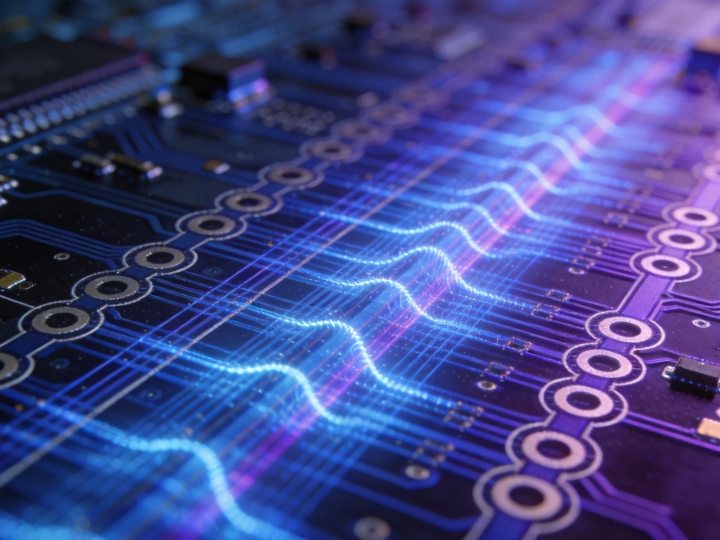
High Frequency PCB Knowledge: Managing Crosstalk and EMI in Dense LayoutsAugust/11/2026
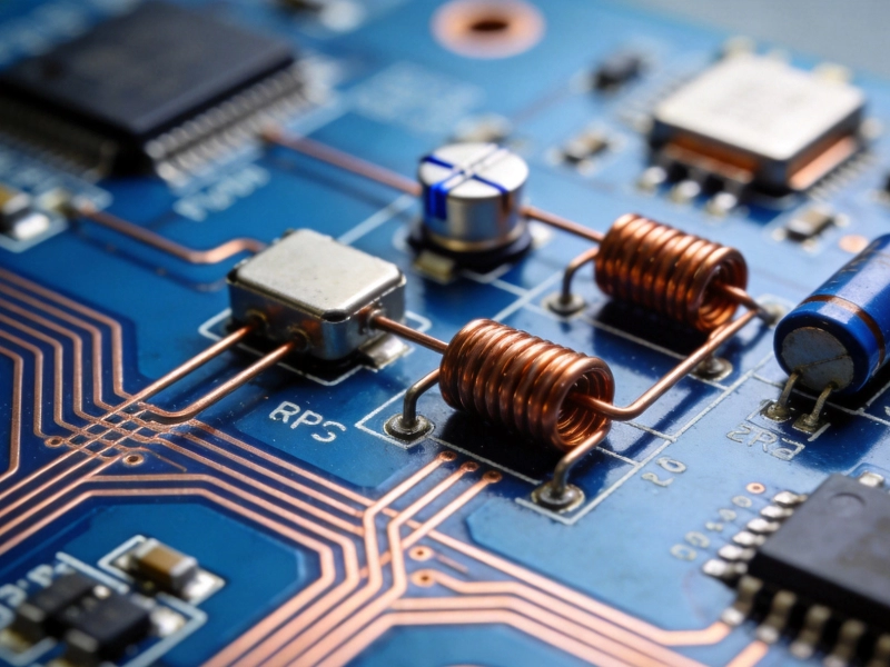
Key High Frequency PCB Knowledge for Successful RF Circuit DesignSeptember/07/2026
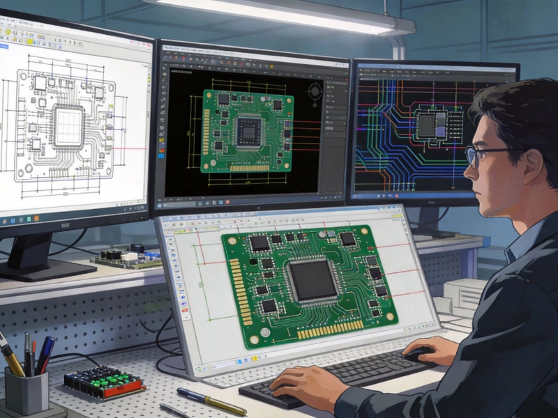
Essential High Frequency PCB Knowledge for Hardware Engineers and DesignersMay/29/2026
High Frequency PCB Knowledge: How to Minimize Insertion Loss and ReflectionJuly/21/2026
Essential High Frequency PCB Knowledge for Hardware Engineers and DesignersJune/15/2026
Demystifying Impedance Control: Core High Frequency PCB KnowledgeJuly/09/2026
SMT vs. THT: Assembly Techniques for High Frequency PCBsJuly/03/2026

High Frequency PCB Capabilities for Aerospace and Defense ApplicationsJuly/17/2026