Open Nav

High Frequency Pcb designs often face a dilemma: the digital section of the board works perfectly well on inexpensive Fr-4 material, but the RF section demands Low-loss Materials that are significantly more expensive. Hybrid stack-ups solve this problem by combining different substrate materials in a single board, placing RF materials where they matter and using standard Fr-4 for the rest. This approach delivers optimal performance where needed without the cost of a full high-frequency board.
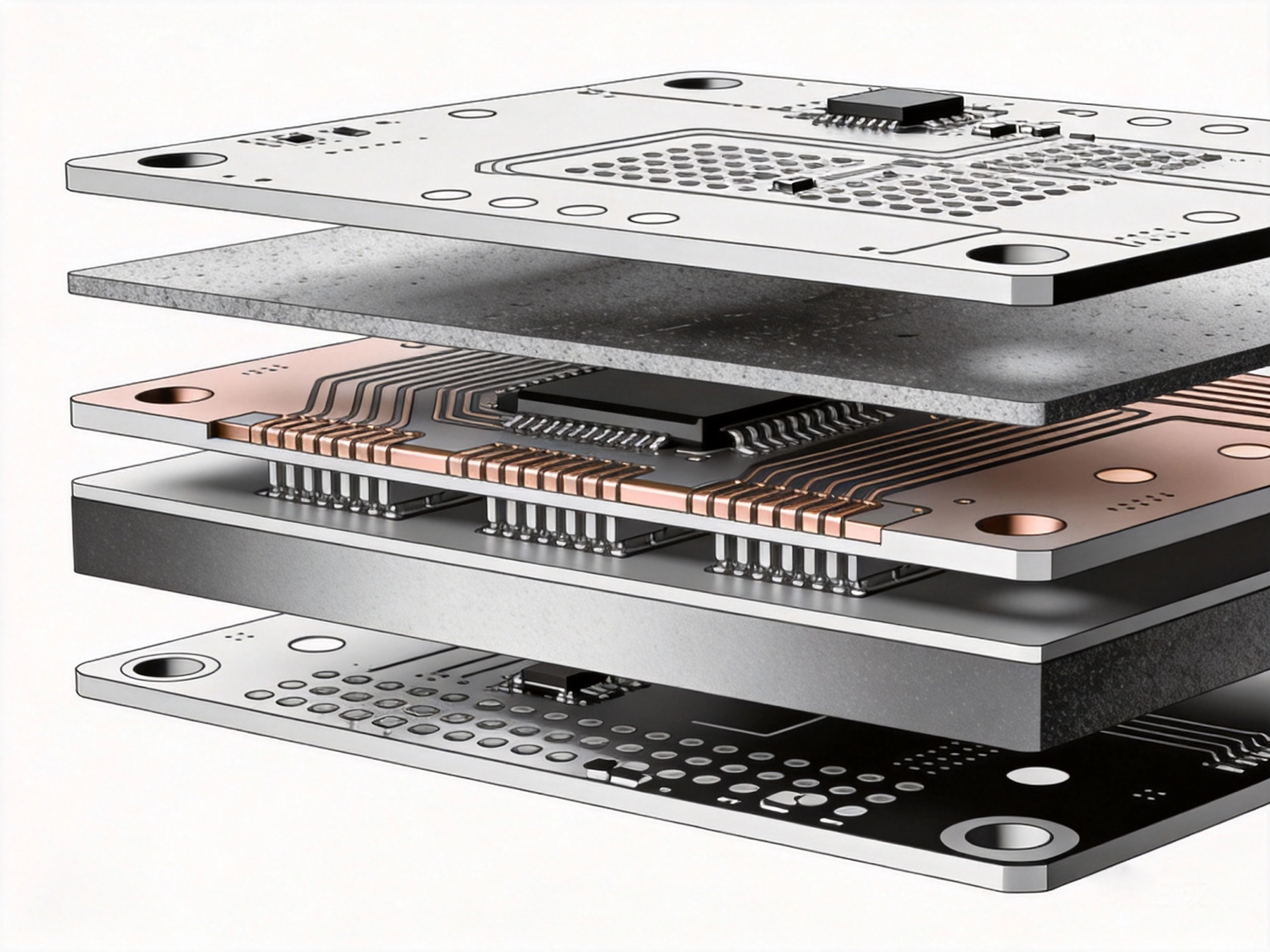
Modern electronics increasingly combine digital processing with RF functionality. A typical example is a board with a processor, memory, and power management running on digital logic, plus a wireless transceiver, antenna matching network, and RF front-end operating at GHz frequencies. The digital section does not require special materials—a standard FR-4 multilayer provides adequate performance at a reasonable cost. The RF section is another matter.
RF signals at 5 GHz and above are sensitive to substrate properties. Standard FR-4 has a Dissipation Factor (Df) around 0.02, which means 2% of the signal energy is lost as heat per wavelength traveled. High-frequency laminates like Rogers RO4003C have Df below 0.004, giving them 5x lower loss at the same frequency. For RF traces carrying signals over meaningful distances on the board, this difference directly affects range, efficiency, and signal quality.
The challenge is that RF materials cost three to ten times more per square inch than FR-4. A board that is 80% digital circuitry should not require 100% RF material cost. Hybrid stack-ups provide a cost-effective solution by using each material where it provides the most value.
A hybrid stack-up uses two or more different substrate materials in the same board. The most common approach places Rf Laminate in the layers that carry RF signals, with FR-4 prepreg bonding the layers together. The stack-up is designed so that the RF signal traces run on the RF material layers, while digital traces run on FR-4 layers.
The key engineering challenge is managing the interfaces between different materials. RF and digital signals must transition between layers through vias, and these transitions must be designed carefully to minimize impedance discontinuities and Signal Integrity problems. The different dielectric constants of FR-4 (typically 4.2–4.5) and RF materials (2.0–3.5) affect trace impedance calculations, so each layer must be modeled with its own material properties.
Thermal expansion is another consideration. FR-4 and RF materials have different coefficients of thermal expansion (CTE), which creates stress at the material boundaries during temperature cycling. This stress is manageable with careful stack-up design and appropriate bonding materials, but it must be accounted for in the material selection and manufacturing process.
The simplest hybrid configuration places a single RF core between two FR-4 prepreg layers. The RF traces run on the outer surfaces of the RF core, while digital traces run on the FR-4 outer layers. This works well for boards with RF traces on the surface, such as antenna feeds and matching networks.
A more complex configuration uses multiple RF cores for designs with buried RF signal layers. This might have RF material as the core with FR-4 buildup layers on both sides. The RF signals are routed on inner layers of the RF core, with digital circuitry on the outer FR-4 layers. This configuration provides more routing flexibility for the RF section but requires more sophisticated modeling to ensure proper transitions.
For designs that need RF on both sides of the board, two RF cores can be used with FR-4 prepreg between them. This creates a symmetric or near-symmetric stack-up that handles thermal stress better than asymmetric configurations.
Several high-frequency laminates are commonly used in hybrid stack-ups. Each has a different balance of electrical performance, thermal properties, and cost.
Rogers RO4003C is a popular choice with Dielectric Constant of 3.38 and Df of 0.0027 at 10 GHz. It is ceramic-filled hydrocarbon composite, less expensive than PTFE-based materials, and compatible with standard FR-4 processing methods. RO4003C is the workhorse for hybrid designs in the 1–20 GHz range, covering Wi-Fi, cellular, and many radar applications.
Rogers Ro4350b is similar to RO4003C but with a Dielectric Constant of 3.48, making it a drop-in replacement for designs that target 50-ohm impedance on standard trace geometries. It is widely supported by PCB fabricators experienced with hybrid work.
For lower frequencies or cost-sensitive applications, Isola I-tera MT40 offers Df of 0.0032 at 10 GHz with the advantage of being halogen-free and RoHS-compliant without special processing. It bridges the gap between standard FR-4 and premium RF materials.
PTFE-based materials like Rogers RT/duroid 5880 provide the lowest loss but require specialized processing—PTFE does not bond with standard FR-4 prepreg, requiring special adhesive films or fusion bonding. The processing complexity and cost make these materials less common in hybrid designs unless the application demands their performance.
The interface between RF and digital sections is the most critical part of a hybrid design. RF signals traveling from a transceiver chip to an antenna must pass through the stack-up, transitioning from the RF material layer to the antenna pad on the board surface. Each transition point is a potential source of impedance mismatch and Signal Loss.
Blind vias connecting RF layers to surface pads must be designed with Controlled Impedance. The via barrel acts as a Transmission Line with its own impedance determined by the via dimensions and the surrounding dielectric. If the via impedance differs significantly from the trace impedance, reflections occur at the transition.
Ground via stitching around RF signal vias reduces unwanted coupling and provides return current paths. Place ground vias within 2–3 mm of the signal via on both sides of the RF layer. The ground vias should connect to the RF ground plane on the same layer as the signal trace.
For high-speed digital signals that transition between layers, similar considerations apply—Controlled Impedance, ground via stitching, and minimized stub length. The difference is that digital signals are less sensitive to loss, so the material transition is less critical than for RF signals.
A hybrid stack-up requires more planning than a single-material design. Each layer must be modeled with its actual dielectric properties, and the impedance calculations must account for the different materials. Most PCB design tools handle individual layer materials, but the interface between different dielectrics may require additional attention.
Start with a clear definition of which signals run on which layers. Identify the RF signals and their routing requirements—their operating frequency, trace length, and whether they need controlled impedance. Group the digital signals by speed and routing complexity.
Work with your fabricator early in the design process. They have experience with hybrid stack-ups and can advise on material availability, minimum geometries their process supports, and any process limitations that affect stack-up design. Sharing your preliminary stack-up with them for review before finalizing the layout prevents manufacturability issues later.
Electromagnetic simulation tools help validate the hybrid design before fabrication. Modeling the RF section with its actual material stack-up and transition geometries identifies impedance problems that can be corrected in the layout rather than requiring a board respin.
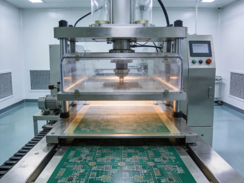
Hybrid stack-ups require process controls beyond standard multilayer fabrication. The different materials have different lamination requirements—temperature, pressure, and time must be balanced to achieve good bond between all layers without damaging any of them.
FR-4 prepreg typically laminates at temperatures around 180–200°C and pressures around 300–400 psi. RF materials like RO4000 series have similar requirements, which makes them compatible with standard FR-4 lamination cycles. This is why these materials are popular for hybrid designs—the processing parameters overlap.
PTFE-based RF materials are less compatible. They require higher lamination temperatures or special adhesive films, which increases complexity and cost. If your design needs PTFE performance, evaluate whether a RO4000 series material can meet your loss requirements before committing to the added processing difficulty.
Drilling and plating parameters must be optimized for the hybrid stack-up. The drill parameters that work well for FR-4 may not be optimal for RF cores, which have different resin systems and reinforcement. Your fabricator's experience with hybrid materials determines how well they manage these parameters.
Hybrid stack-ups are worth the added complexity when your design has a clear separation between RF and digital functions, when the RF section represents less than half the board area, and when signal frequencies are high enough that FR-4 loss is a concern.
Typical applications include Wi-Fi and Bluetooth modules with integrated processors, cellular IoT devices with RF transceivers and digital baseband, radar modules with RF front-ends and digital signal processing, and test equipment with RF measurement circuits and digital display and control sections.
If your entire board is RF—say, a pure 77 GHz radar sensor—a hybrid stack-up offers less benefit because the cost reduction from using FR-4 elsewhere does not apply. In those cases, a homogeneous high-frequency board may be simpler and more cost-effective despite the higher material cost.
The decision also depends on volume. At low volumes, the added fabrication cost of a hybrid stack-up may not be justified by the material savings. At high volumes, the material cost reduction compounds across thousands of boards and typically justifies the more complex manufacturing process.
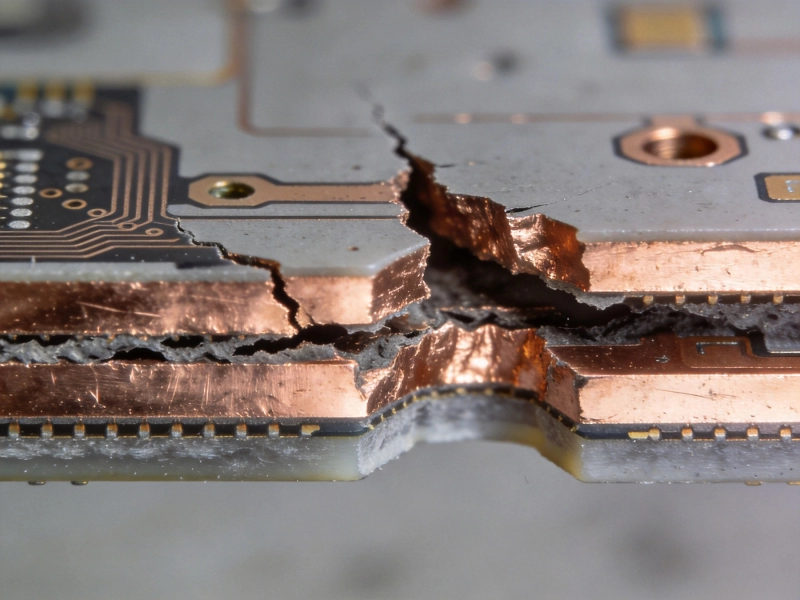
Overcoming Delamination Challenges in Multilayer High Frequency PCB FabricationJuly/28/2026
High Frequency PCB Fabrication with Rogers and PTFE Materials: A Technical GuideJuly/16/2026
Advanced High Frequency PCB Fabrication Techniques for Low Loss PerformanceMay/29/2026
Laser Drilling and Microvias in Modern High Frequency PCB FabricationJuly/07/2026
High Frequency PCB Fabrication Tolerances: Why Precision Matters More Than EverSeptember/02/2026
High Frequency PCB Fabrication: Managing Dielectric Constant (Dk) TolerancesJune/09/2026
The Impact of Surface Roughness on High Frequency PCB Fabrication QualityJune/27/2026
The Role of Vacuum Lamination in High Frequency PCB FabricationAugust/07/2026