Open Nav

Delamination — the separation of copper layers from dielectric material or the separation of dielectric layers from each other — is one of the most destructive failure modes in multilayer Pcb Fabrication. A board that looks perfect on the surface can harbor internal delamination that opens circuits, creates impedance discontinuities, and allows moisture ingress that accelerates corrosion. For high-frequency designs where Controlled Impedance and Signal Integrity are essential, delamination is a show-stopper.
This article examines why delamination occurs in multilayer high-frequency PCBs, how to detect it, and what fabrication practices prevent it. The focus is on practical solutions that work in production, not just theoretical material science.
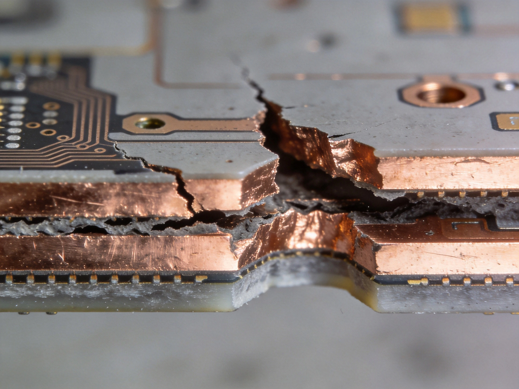
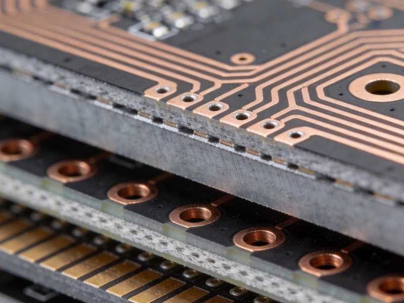
Delamination is a separation at an interface. In multilayer PCBs, that interface is typically between copper and prepreg, between prepreg and core laminate, or between layers in a sequential build-up construction. The separation can be partial — a small bubble or void — or it can extend across a significant area of the board.
Delamination is not always visible from the surface. Internal delamination may only be detectable through cross-section analysis or electrical testing. A board can pass visual inspection and impedance testing, then fail in the field when thermal cycling or moisture exposure causes a marginal bond to separate completely.
The consequences of delamination depend on where it occurs and how the board is used. Delamination under a controlled-impedance trace changes the effective Dielectric Constant and creates an impedance discontinuity. Delamination under a via barrel can open the connection entirely. Delamination at a ground plane interface creates electrical noise paths that degrade Signal Integrity. In high-frequency applications, any of these effects can cause system-level failure.
Understanding the causes is the first step to prevention. Delamination in multilayer high-frequency PCBs typically results from one or more of these factors.
The lamination process bonds layers together under heat and pressure. If the temperature profile, pressure, or time are insufficient, the resin in the prepreg may not fully flow and wet the copper surfaces. Incomplete wetting creates weak interfaces that are prone to separation.
High-frequency materials often have different lamination requirements than standard Fr-4. PTFE-based materials, ceramic-filled laminates, and modified epoxy systems each have specific temperature and pressure profiles that must be followed. Using a generic lamination recipe for these materials is a common cause of delamination.
Different materials expand at different rates when heated. The coefficient of thermal expansion (CTE) mismatch between copper and dielectric, or between different dielectric layers, creates stress during temperature changes. If the bond strength at the interface is insufficient to resist this stress, delamination occurs.
High-frequency designs often combine different material types — for example, a PTFE-based layer for RF signals and Fr-4 for control circuits. These hybrid stack-ups require careful material selection to minimize CTE mismatch and ensure reliable bonding.
Many high-frequency materials are more hygroscopic than standard FR-4. Moisture absorbed into the dielectric expands rapidly when the board is heated during lamination or assembly. The resulting steam pressure can literally blow apart the bond between layers.
Moisture-related delamination often appears as small bubbles or voids scattered through the board cross-section. The effect may not be visible until the board goes through reflow soldering, when the higher temperatures cause absorbed moisture to vaporize and create pressure at the interfaces.
Any contamination on copper surfaces or prepreg material interferes with bonding. Oxidation, fingerprints, dust, or release agents can prevent proper adhesion during lamination. Clean handling procedures and proper storage conditions for materials are essential for preventing contamination-related delamination.
Lead-free soldering requires higher peak temperatures than tin-lead solder. For some material combinations, the thermal stress of lead-free assembly exceeds the bond strength at certain interfaces. Boards that survive fabrication may delaminate during assembly if the material selection and process parameters are not matched.
Detection methods range from visual inspection to advanced analysis techniques. The appropriate method depends on the stage of production and the criticality of the application.
Surface delamination can sometimes be seen as a whitening or bubbling of the laminate surface. However, internal delamination is invisible from the surface. Cross-section analysis — cutting a sample, potting it in epoxy, polishing the face, and examining under a microscope — reveals internal delamination. This is a destructive test, so it is typically performed on coupons or first articles rather than production boards.
Opens and shorts testing can detect delamination that has caused circuit interruptions. However, a delamination that has not yet caused a complete separation may not be detected electrically. Impedance testing can reveal impedance discontinuities that suggest internal delamination, but interpretation requires correlation with physical analysis.
Thermal cycling and thermal shock testing can induce delamination in boards that have marginal bond strength. This is a screening test — boards that survive thermal stress testing are more likely to remain intact in service. For high-reliability applications, thermal stress testing is part of qualification and acceptance testing.
Scanning acoustic microscopy (SAM) uses ultrasonic waves to detect internal delamination non-destructively. Delaminated regions reflect ultrasound differently than bonded regions, creating contrast in the image. SAM can map delamination across an entire board without destructive sample preparation. This technique is used for critical applications where internal delamination must be detected without destroying the board.
Preventing delamination requires attention throughout the fabrication process, from material selection through final inspection.
Select materials with proven compatibility. When combining different material types in a hybrid stack-up, verify that the materials bond reliably together. Consult material manufacturer recommendations for lamination parameters and process windows. Do not assume that materials from different suppliers will bond reliably without qualification testing.
For high-frequency designs, choose materials with low moisture absorption and proven performance under lead-free assembly conditions. The material data sheet should specify moisture absorption characteristics and recommended storage conditions.
Store prepreg and laminate materials under controlled humidity and temperature conditions. Many materials require storage in moisture-barrier bags or humidity-controlled environments. Follow the material manufacturer's storage recommendations exactly.
Limit exposure time between removing materials from controlled storage and lamination. Some materials begin absorbing moisture within hours of exposure. Track exposure time and bake materials if exposure limits are exceeded.
Baking prepreg and laminate before lamination removes absorbed moisture. The bake temperature and time depend on the material and the exposure history. A typical bake might be 125 degrees Celsius for 4 to 8 hours, but follow material manufacturer recommendations. Baking does not help if the material has already absorbed excessive moisture — some materials cannot be fully dried once contaminated.
Use lamination parameters appropriate for the specific materials. Temperature ramp rate, hold time, pressure profile, and cooling rate all affect bond quality. High-frequency materials often require slower ramp rates to allow uniform heating of materials with different thermal properties.
Work with your fabricator to confirm that their lamination process matches the material requirements. For hybrid stack-ups, the lamination parameters must work for all materials in the stack, which may require compromise between optimal parameters for each material.
Implement clean room or clean area procedures for handling prepreg and laminate. Avoid touching copper surfaces with bare hands. Use gloves that do not leave residue. Keep materials covered when not in use. Follow handling procedures that minimize contamination.
Match the assembly thermal profile to the material capabilities. For materials with marginal thermal resistance, consider using a lower-temperature solder profile or limiting the number of reflow passes. Conformal coating can provide additional protection against moisture ingress that could cause delamination in service.
Design choices influence delamination susceptibility. These practices reduce risk.
Large copper areas on one layer with no corresponding copper on adjacent layers create asymmetric stress during lamination and thermal cycling. The differential expansion between copper-heavy and copper-free areas concentrates stress at the interface. Design with balanced copper distribution or add copper balancing to even out the distribution.
Sharp corners in copper features can concentrate stress during thermal cycling. Use rounded corners where possible, especially for large copper areas. Avoid designing copper features that create stress concentrations at layer interfaces.
Sequential lamination — laminating a subset of layers, then adding more layers in a second lamination cycle — adds thermal cycles to the inner layers. Each thermal cycle adds stress to the interfaces. For delamination-sensitive applications, consider whether sequential lamination is necessary or whether a single lamination cycle can achieve the required construction.
Delamination prevention is a collaboration between designer and fabricator. These practices improve outcomes.
Communicate your application requirements clearly. If the board will be exposed to high-temperature assembly or harsh environmental conditions, the fabricator needs to know. This information affects material recommendations and process controls.
Request cross-section analysis on first articles. This verifies that the lamination process is producing well-bonded boards. If delamination is found, address it before proceeding to production.
Ask about your fabricator's process controls for moisture management, lamination parameters, and material qualification. A fabricator with robust process controls is more likely to produce delamination-free boards.
For critical applications, consider specifying thermal stress testing or acoustic microscopy inspection as part of acceptance criteria. These tests add cost but provide confidence that boards are free of internal delamination.
Generally, no. Delamination is a separation at the material interface that cannot be reliably re-bonded. The board may function initially after rework, but the interface remains weakened and will likely fail under thermal or mechanical stress. For high-reliability applications, delaminated boards should be scrapped and replaced.
Materials with high moisture absorption, such as some PTFE-based laminates and polyimide, are more susceptible to moisture-induced delamination. Materials with high CTE or significant CTE mismatch with copper create more thermal stress during temperature cycling. Material selection should consider these factors for delamination-sensitive applications.
Visual inspection cannot detect internal delamination. Cross-section analysis is the definitive method — it shows the actual bond line between layers. For non-destructive detection, scanning acoustic microscopy can reveal internal delamination without destroying the board. Electrical testing may detect the effects of delamination but cannot confirm the presence of delamination directly.
No. A partial delamination may not cause any electrical symptom initially. The board may pass functional testing. However, delamination creates a weakened interface that can propagate under thermal cycling, vibration, or moisture exposure. A board that works at initial acceptance may fail in service weeks or months later.
For high-reliability applications, specify thermal cycling that exceeds the expected service conditions. A common specification is IPC-TM-650 method 2.6.7, which subjects boards to temperature cycling between -40 degrees Celsius and +125 degrees Celsius. The number of cycles depends on the application. For critical applications, 100 cycles or more may be specified. Ensure that the material selection and lamination process are qualified to survive the specified testing.
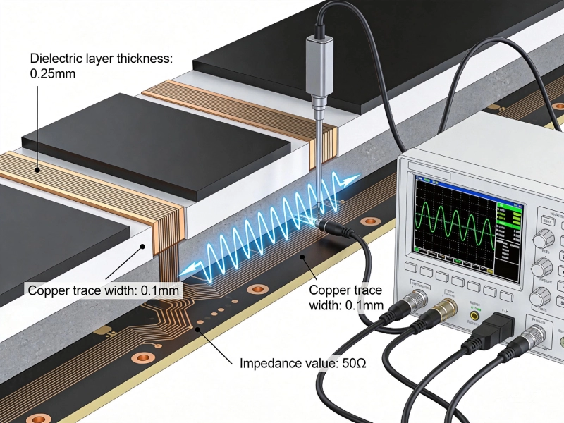
High Frequency PCB Fabrication: Managing Dielectric Constant (Dk) TolerancesJune/09/2026
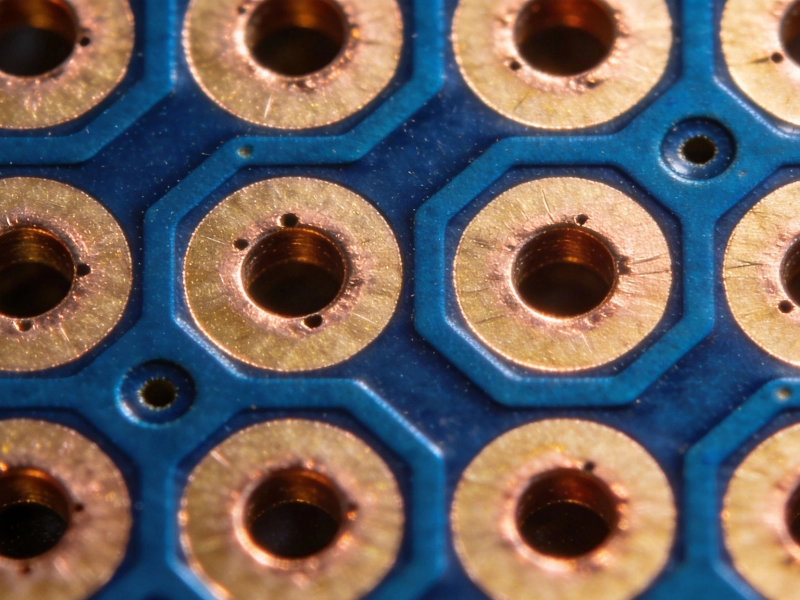
Laser Drilling and Microvias in Modern High Frequency PCB FabricationJuly/07/2026
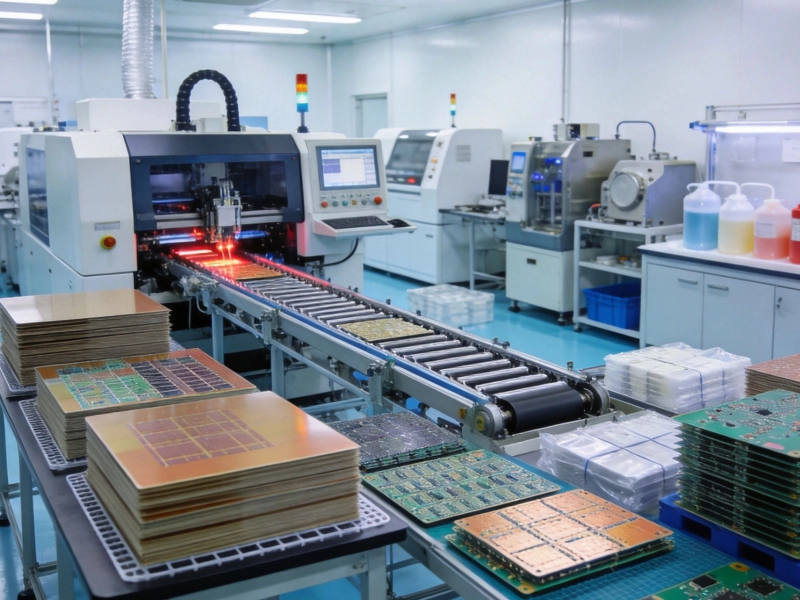
Advanced High Frequency PCB Fabrication Techniques for Low Loss PerformanceMay/29/2026
The Impact of Surface Roughness on High Frequency PCB Fabrication QualityJune/27/2026
High Frequency PCB Fabrication Tolerances: Why Precision Matters More Than EverSeptember/02/2026
The Role of Vacuum Lamination in High Frequency PCB FabricationAugust/07/2026
High Frequency PCB Fabrication with Rogers and PTFE Materials: A Technical GuideJuly/16/2026
Understanding Thermal Stability in High Frequency PCB MaterialsAugust/10/2026