Open Nav

High frequency printed circuit boards serving RF and microwave applications demand fabrication precision exceeding that of standard digital boards. Signal Loss, impedance variation, and reliability failures in high frequency circuits often trace to fabrication inconsistencies that would be insignificant in lower-frequency designs. Vacuum lamination represents a critical process step where these inconsistencies originate, yet this essential operation receives less attention than it deserves. Understanding how vacuum lamination influences high frequency PCB quality helps designers specify appropriate requirements and fabricators optimize their processes for RF applications.
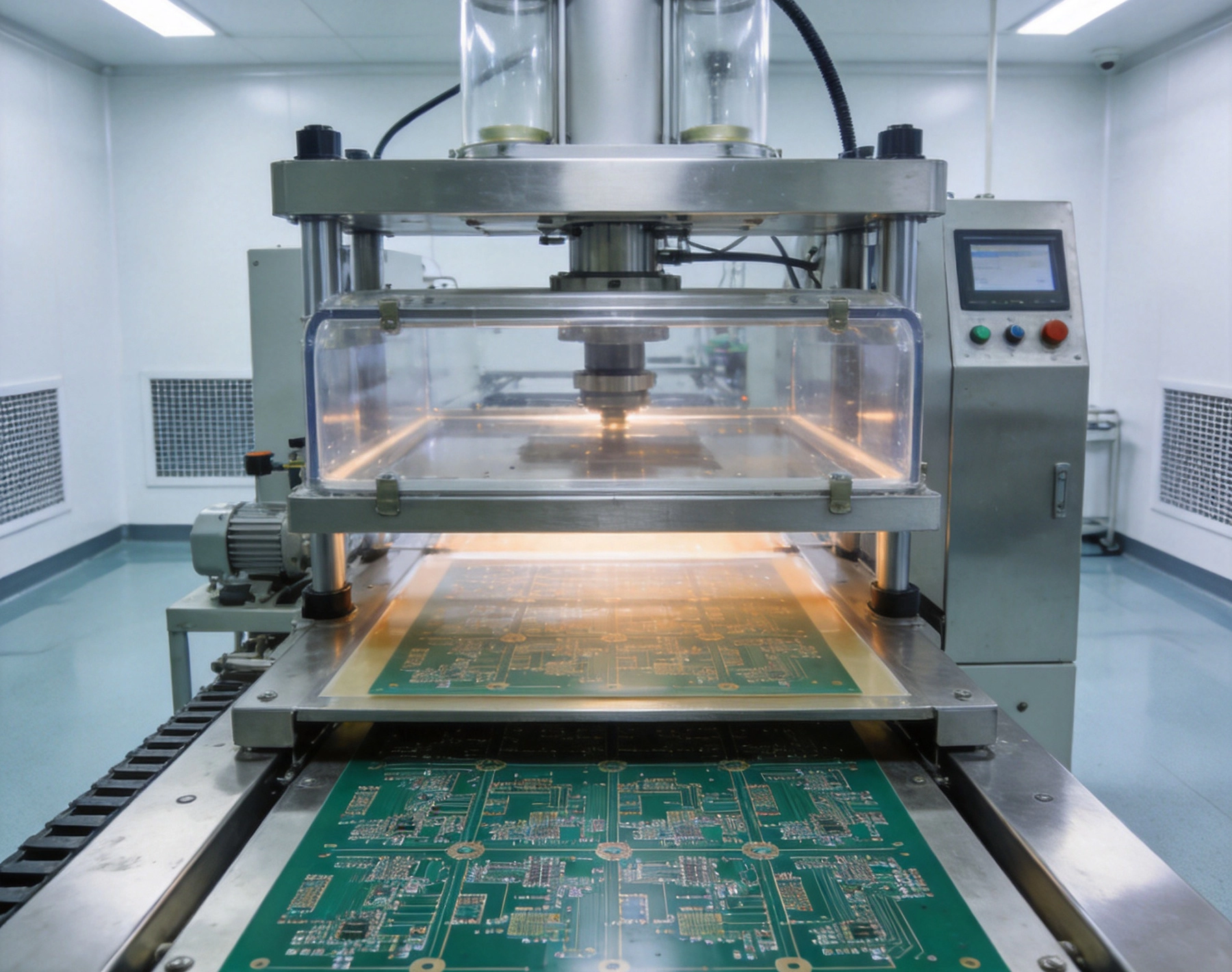
Multilayer PCB construction requires bonding individual circuit layers into unified structures capable of surviving drilling, plating, and thermal stress throughout operational life. The lamination process applies heat and pressure to melt prepreg sheets sandwiched between copper-clad layers, creating solid dielectric layers that insulate and separate conductor patterns. This bonding operation fundamentally influences final board quality across all performance categories.
Standard lamination uses hydraulic presses that apply pressure from above and below the board stack. While adequate for many applications, this approach creates inherent challenges that vacuum lamination addresses. The pressure medium in standard lamination includes both hydraulic fluid and trapped air, creating pressure variations across the board surface that affect resin flow and void formation.
Vacuum lamination encloses the board stack within sealed membranes before applying pressure, using atmospheric pressure rather than mechanical force to achieve bonding. This approach eliminates pressure medium contamination while enabling more uniform pressure distribution. For boards where consistency matters, these differences translate directly into quality improvements.
Voids within laminate dielectric layers create problems that scale with operating frequency. At low frequencies, small voids might cause no observable performance degradation. At microwave frequencies where wavelengths shrink to millimeters, void-induced impedance variations produce signal reflections and loss that accumulate across circuit paths.
The Dielectric Constant of air differs significantly from that of cured prepreg. When voids occupy any meaningful volume fraction, the effective Dielectric Constant varies from design targets, causing impedance deviations that degrade Signal Integrity. Even small voids create measurable effects in 5G millimeter-wave applications where tolerances approach ±0.5%.
Vacuum lamination dramatically reduces void formation by removing air from the bond line before pressure application. The vacuum environment expands gas volumes, pulling them from developing bond lines before resin flow seals them in place. This bubble removal capability makes vacuum lamination nearly essential for demanding high frequency applications.
Prepreg resin must flow sufficiently to fill gaps between copper features and create continuous dielectric layers. Insufficient flow leaves voids around tall copper features. Excessive flow thins dielectric layers below designed thickness or pushes resin away from critical areas. Controlled resin flow determines final dielectric thickness and composition.
Vacuum assistance enables more controlled resin flow than standard press lamination. By reducing external pressure while maintaining vacuum within the membrane, operators can arrest resin flow at precise points during the bonding cycle. This control proves valuable for thick boards with significant copper topography requiring consistent dielectric layers across varying feature densities.
Flow uniformity across large panels affects production yields and performance consistency. Standard lamination produces subtle thickness variations that might be acceptable for digital circuits but problematic for distributed element circuits where dimensional tolerances directly influence electrical performance. Vacuum lamination produces more consistent results across larger board areas.
Multilayer boards require precise alignment between layers separated by Dielectric Materials. Registration errors shift conductor positions from design targets, causing impedance variations that compound across multiple layers. High density interconnect designs with fine trace widths and tight spacing demand registration precision that standard lamination struggles to achieve consistently.
Vacuum lamination applies uniform pressure that pulls layers toward tooling reference points more effectively than standard press lamination. The atmospheric pressure acts equally across the entire panel surface, maintaining layer alignment throughout the bonding cycle. This pressure uniformity reduces layer shift that can occur when pressure application creates movement before resin gels.
Inner layer imaging alignment tolerances of ±0.05mm or tighter require process control throughout subsequent operations. Lamination should not introduce errors that exceed half of the allocated tolerance budget. Vacuum lamination contributes to maintaining registration within these demanding specifications.
High frequency laminates from manufacturers like Rogers, Taconic, and Isola contain specialized dielectric formulations optimized for RF performance. These materials may include ceramic fillers, Ptfe compositions, or glass reinforcement that behave differently from standard Fr-4 during lamination. Vacuum lamination accommodates these variations more gracefully than standard processes.
Ptfe-based laminates present particular lamination challenges due to their nonstick properties. Resin flow characteristics differ from thermosetting prepregs, requiring modified bonding approaches. Vacuum lamination provides the pressure uniformity and void elimination that PTFE constructions demand for reliable bonding.
Thermal compression during lamination must not degrade the electrical properties that distinguish High Frequency Materials. Excessive temperature or pressure can alter filler distributions or cause resin squeeze-out that changes effective dielectric constant. Vacuum lamination's controlled pressure application reduces risk of these property changes.
Vacuum-assisted lamination encompasses several specific approaches with different characteristics. Full vacuum lamination encloses the entire press area within vacuum chambers, achieving the most complete air removal. Vacuum bag lamination applies membranes directly to board stacks within the press, achieving most vacuum benefits at lower equipment cost.
Vacuum press systems dedicated to High Frequency Materials offer process optimization that general-purpose equipment cannot match. Temperature profiles, pressure ramps, and vacuum levels can be tuned specifically for High Frequency Laminate requirements. This specialization improves consistency and yield for demanding applications.
Standard hydraulic press lamination without vacuum assistance may be acceptable for some high frequency applications where cost constraints limit options. Boards with thicker dielectrics, lower frequency operation, or generous performance margins might achieve adequate quality. However, specifying vacuum lamination ensures that process limitations do not constrain achievable performance.
Vacuum lamination success depends on proper setting of temperature, pressure, vacuum level, and timing parameters. Each laminate material has recommended processing windows that vary based on thickness, copper weight, and panel size. Optimization within these windows determines final quality and production throughput.
Vacuum level during lamination directly influences void elimination. Higher vacuum levels remove more air but require longer pump-down times. Process engineering balances vacuum effectiveness against cycle time requirements. For most high frequency applications, vacuum levels below 10 mbar provide adequate void elimination.
Heating rate affects resin flow timing relative to void removal. Slow heating allows more time for vacuum application before gelation begins. Fast heating reduces cycle time but might trap voids before evacuation completes. Understanding material rheology guides appropriate heating rate selection.
Verifying lamination quality requires inspection methods that detect internal defects invisible to visual examination. Ultrasonic scanning acoustic microscopy (SAM) images internal layer interfaces, revealing voids, delaminations, and resin distribution variations. This non-destructive technique provides comprehensive quality verification for critical applications.
Cross-section analysis destructively samples boards to reveal internal structure. Microsectioning along critical signal paths verifies that dielectric thickness and composition meet specifications. This verification confirms that lamination processes produce designed electrical characteristics.
Electrical testing complements physical inspection by verifying that fabricated boards meet RF performance targets. Impedance measurements at multiple points confirm manufacturing consistency. Time domain reflectometry reveals impedance discontinuities that might indicate internal defects.
Insertion Loss in high frequency circuits combines conductor losses, dielectric losses, and radiation losses. Dielectric Loss Factor (Df) often dominates at higher frequencies, but void content within Dielectric Materials can increase effective loss beyond material specifications. Vacuum lamination's void elimination helps achieve designed loss performance.
The quality factor (Q) of resonators and filters correlates directly with dielectric loss. Voids in high Q structures create loss variations that degrade filter skirts and reduce resonator Q. Vacuum lamination's consistent void-free bonding enables the high Q performance that advanced RF applications demand.
5G millimeter-wave applications operating at 28 GHz and above face Insertion Loss budgets that demand every fabrication improvement. The difference between standard and vacuum lamination might contribute several tenths of a dB improvement that proves decisive in achieving system link budgets.
High Frequency Laminate materials vary in their compatibility with standard PCB Fabrication processes including lamination. Some specialized materials require modified processing to achieve designed properties. Consulting with material suppliers and experienced fabricators early in design helps identify potential process conflicts.
Ceramic-filled laminates provide excellent high frequency performance but may require higher lamination pressures or temperatures than standard prepregs. The filler materials can settle during processing, creating non-uniform dielectric properties if process controls do not compensate. Vacuum lamination's pressure uniformity helps maintain filler distribution.
Low-flow prepregs designed for thick constructions may not flow adequately in standard lamination. Vacuum assistance can help these materials achieve adequate bonding without excessive flow. Material data sheets typically specify recommended processing approaches for different constructions.
Vacuum lamination equipment represents significant capital investment, with dedicated systems costing considerably more than standard presses. This investment reflects in pricing for vacuum-laminated boards, creating cost premiums that must be justified against performance benefits.
For applications where high frequency performance directly determines product viability, vacuum lamination cost premiums may be trivial compared to performance improvements. Antenna arrays, radar systems, and high-performance filters often justify premium processing to achieve designed electrical characteristics.
Lower-performance applications might achieve acceptable results with standard lamination, avoiding unnecessary cost premiums. Understanding performance requirements enables appropriate process selection that balances cost against achievable performance.
Process monitoring and control technologies continue advancing vacuum lamination capabilities. Real-time temperature and pressure monitoring within vacuum chambers enables closed-loop control that improves consistency. These advances reduce variation that affects high frequency performance.
Alternative bonding approaches including laser bonding and adhesive bonding may eventually challenge traditional lamination methods. These emerging technologies offer potential advantages for specific applications but currently lack the maturity and cost-effectiveness for widespread adoption.
Materials development continues creating laminates with improved high frequency properties. Processing requirements for these advanced materials will drive corresponding advances in lamination technology to achieve designed performance.
Vacuum lamination provides essential quality improvements for high frequency PCB Fabrication. The void elimination, pressure uniformity, and resin flow control that vacuum technology enables address the fabrication challenges that limit high frequency performance. Understanding these benefits guides appropriate process specification and fabricator selection.
Successful high frequency PCB fabrication requires collaboration between designers understanding electrical requirements and fabricators mastering lamination processes. This partnership ensures that designs translate into products achieving intended performance. The investment in quality lamination processes yields returns through reliable high frequency products.
As RF and microwave applications continue expanding into 5G, Automotive Radar, and advanced communications, demand for high quality laminated boards will intensify. Vacuum lamination capabilities position fabricators to serve these demanding markets while enabling products that perform reliably throughout their operational lives.
The Impact of Surface Roughness on High Frequency PCB Fabrication QualityJune/27/2026
Overcoming Delamination Challenges in Multilayer High Frequency PCB FabricationJuly/28/2026
High Frequency PCB Fabrication with Rogers and PTFE Materials: A Technical GuideJuly/16/2026
High Frequency PCB Fabrication Tolerances: Why Precision Matters More Than EverSeptember/02/2026
Hybrid Stack-ups: Combining FR4 and RF Materials in High Frequency PCB FabricationSeptember/14/2026
Laser Drilling and Microvias in Modern High Frequency PCB FabricationJuly/07/2026
Environmental Considerations in Sustainable High Frequency PCB FabricationSeptember/23/2026
High Frequency PCB Fabrication: Managing Dielectric Constant (Dk) TolerancesJune/09/2026