
When signal frequencies climb past a few gigahertz, the properties of Pcb Materials stop being background physics and start being the primary determinants of circuit performance. At 10 GHz, a dielectric that behaves perfectly fine at 100 MHz can introduce enough signal distortion to make your receiver design unworkable. The two material parameters that matter most at these frequencies are Dielectric Constant—how much the material stores electrical energy—and Loss Factor—how much energy the material dissipates as heat.
I've spent years selecting materials for RF and high-speed digital applications, and the most common mistake I see is treating Dk and Df as fixed values. They're not. Both parameters shift with frequency, temperature, and humidity in ways that can dramatically affect your circuit's behavior. Understanding these dependencies separates designs that work in the lab from designs that work in the field.
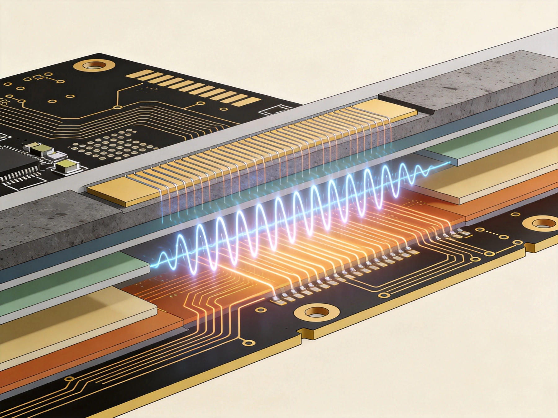
Dielectric Constant, also called relative permittivity and symbolized as Dk or Er, describes how much the material amplifies the capacitance between conductors. In free space, the value is exactly 1.0. Most Pcb Materials fall between 2.8 and 6.5, meaning they increase capacitance by that factor compared to air. This sounds simple, but the practical implications are substantial.
For Transmission Lines, Dk determines the speed at which signals propagate. The relationship is inverse—higher Dk means slower signal velocity. A Microstrip on Fr-4 with Dk of 4.5 propagates signals at about half the speed of light. The same geometry on Ptfe with Dk of 2.1 propagates at roughly 70% of light speed. This velocity difference affects everything from Impedance Matching to delay in high-speed digital interconnects.
The more critical implication for Rf Design is dimensional consistency. When your circuit is designed for a specific Dk value, manufacturing variation in that Dk directly affects impedance and resonant frequency. If the material you specified has Dk tolerance of plus or minus 0.1 and your design sensitivity is 50 ohms per Dk unit, you might be looking at impedance tolerances that exceed your specification by a factor of two or more. Rf Circuits with resonant elements—filters, oscillators, couplers—are particularly vulnerable because frequency accuracy depends directly on Dk.
The Dk value published in material datasheets is typically measured at a specific frequency, often 1 MHz or 10 GHz. But Dk doesn't stay constant across frequency ranges. Most PCB materials exhibit dispersion—Dk decreases as frequency increases. The effect is most pronounced in the transition from low frequencies where dipole relaxation effects dominate to microwave frequencies where electronic polarization dominates.
Ptfe-based materials show relatively flat Dk behavior across broad frequency ranges, making them predictable for wideband applications. Fr-4 and other epoxy-glass materials can exhibit Dk variation of 5-10% between 1 GHz and 10 GHz. This variation sounds modest until you calculate its effect on phase length in a 77 GHz Automotive Radar application, where a few percent length error translates directly to angle error in the radar's field of view.
When selecting materials for wideband applications, look for datasheets that specify Dk at multiple frequencies across your operating range. The variation trend matters as much as the absolute values—if Dk decreases predictably with frequency, you can model the behavior. If the datasheet only provides a single-point specification, ask the manufacturer for additional characterization data or test coupons that let you measure the actual material behavior in your application.
Loss Factor, formally called Dissipation Factor and abbreviated as Df or tan delta, measures how efficiently a dielectric material converts electrical energy into heat. Lower Df means less energy loss. For most PCB applications, this loss is negligible. At high frequencies, it becomes the dominant performance limitation.
Signal attenuation from dielectric loss accumulates with distance and frequency. A Transmission Line with 3 dB attenuation per inch at 10 GHz loses half the signal power across a one-inch run. The same line at 5 GHz might lose only 1 dB. The frequency-squared relationship means that as you push into millimeter-wave frequencies—30 GHz and above—dielectric loss quickly dominates over conductor loss as the primary signal degradation mechanism.
The loss tangent definition—tan(delta) where delta is the phase angle between capacitive and resistive current—creates a useful mental model. Imagine current flowing through a capacitor. Perfect dielectric: current leads voltage by exactly 90 degrees. Real dielectric: current leads by slightly less than 90 degrees. The angular shortfall, delta, multiplied by the frequency gives you the loss. The tangent of delta—the ratio of resistive to capacitive current—is the Dissipation Factor.
Different material families have dramatically different Df values. Standard FR-4 typically exhibits Df of 0.02 or higher at microwave frequencies—losing 2% of signal energy per cycle. High-performance Rf Materials like Rogers Ro4003c have Df around 0.0027—about ten times better. Aerospace-grade PTFE laminates can achieve Df below 0.001. For long transmission runs or millimeter-wave frequencies, this difference translates directly to link budget margins.
Dk and Df are related but not directly proportional. Some materials achieve low loss without extreme Dk values. PTFE has low Df and moderate Dk around 2.1—favorable for many RF applications. Ceramic-filled PTFE materials push Dk higher to 6-10 while maintaining low Df, trading velocity for thermal stability. Hydrocarbon ceramics like Rogers Ro4350b sit in the middle with Dk around 3.5 and Df around 0.003.
The tradeoff between Dk and processability also shapes material selection. PTFE is notoriously difficult to process—it's chemically inert, melts at high temperatures, and requires special handling for plating and machining. Hydrocarbon ceramic materials bridge the gap by providing PTFE-like electrical properties with FR-4-like process compatibility. They bond with standard prepreg, drill and plate like standard materials, and survive standard Pcb Assembly temperatures without special handling.
For high-layer-count designs, FR-4 layers mixed with high-performance RF layers create hybrid stackups that balance cost and performance. Digital layers on FR-4 handle the control logic and power distribution while RF layers on specialized material carry the high-frequency signals. The interface between material types requires careful management—routing signals between layers of different Dk changes impedance abruptly—but the cost savings often justify the complexity.
Temperature variation affects both Dk and Df in ways that matter for outdoor or industrial applications. Most PCB materials have positive temperature coefficients for Dk—Dk increases as temperature rises. The coefficient is typically expressed in parts per million per degree Celsius and can range from 50 ppm/°C for stable materials to over 200 ppm/°C for standard FR-4.
For wide temperature range applications, this Dk shift creates performance drift. An oscillator circuit designed for 24 GHz at room temperature might drift to 23.7 GHz at -40°C and 24.3 GHz at +85°C. For consumer applications, this drift might be acceptable. For automotive safety systems operating across the full vehicle temperature range, the drift must be accounted for in the frequency plan and budget.
Some materials offer controlled thermal expansion coefficients that help manage the interaction between thermal drift and mechanical stability. Ceramic-filled materials provide better dimensional stability across temperature than pure PTFE, reducing the mechanical stress on plated through-holes and via barrels during thermal cycling. The tradeoff is typically higher Dk and slightly higher Df than unfilled materials.
Df variation with temperature tends to be less dramatic than Dk variation, but can still matter at millimeter-wave frequencies. High-humidity conditions amplify temperature effects—moisture absorbed by the dielectric changes both Dk and Df, and the absorbed moisture has its own temperature coefficients. Sealed or coated assemblies that exclude moisture eliminate this variable for most applications.
Water has Dk of about 80 and Df of 0.1 at low frequencies—orders of magnitude worse than any PCB laminate. Even small amounts of moisture absorbed into the dielectric dramatically shift both parameters. FR-4 can absorb 0.1-0.2% moisture by weight under standard conditions, and each 0.01% moisture increase might shift Dk by 0.01 and Df by 0.001. In high-humidity environments or for water-absorbing materials like some polyimides, the effect can be much larger.
The practical consequence for Rf Design is humidity sensitivity. A filter designed in Phoenix in February with 20% relative humidity might perform differently in Singapore in August at 90% relative humidity. The moisture shifts dielectric properties and changes impedance and frequency response. For outdoor infrastructure, marine applications, or tropical deployments, moisture effects must be part of the design budget.
Conformal Coating or full encapsulation helps but introduces its own variables. The coating material has its own Dk and Df, and its effect on the circuit depends on thickness and coverage. A thin conformal coat over RF features might slightly modify field distribution without major impact. Thick encapsulation with a high-Dk material can significantly shift impedance and frequency response. Test coated assemblies against uncoated performance to validate coating effects before committing to production.
For applications below 6 GHz, standard high-Tg FR-4 often suffices if your impedance and loss budgets are generous. Many Wi-Fi, Bluetooth, and cellular applications in the sub-6 GHz range work fine on FR-4, particularly for short trace lengths where accumulated loss remains manageable. The cost advantage is substantial—FR-4 materials cost a fraction of specialty RF laminates.
Between 6 GHz and 20 GHz, the argument for specialized materials strengthens considerably. The loss advantage of low-Df materials becomes meaningful, and Dk variation across frequency becomes harder to ignore. Rogers Ro4350b, Isola Itera, and similar hydrocarbon ceramic materials provide the right balance of electrical performance and process compatibility for most applications in this range.
Above 20 GHz—millimeter-wave frequencies for 5G FR2, Automotive Radar, and Satellite Communications—specialized PTFE or ceramic-filled PTFE materials become necessary for most designs. The loss and stability requirements at these frequencies exceed what hybrid organic materials can deliver. Rogers RT/duroid, Arlon CuFlon, and similar materials set the baseline for this frequency range, though the cost and manufacturing complexity are substantially higher than organic materials.
Your specific application determines which parameters matter most. A narrowband filter might prioritize Dk consistency across temperature to maintain frequency accuracy. A long RF feed line prioritizes Df to minimize loss. A wideband sensor application might need both stable Dk and low Df across a broad frequency range. Understanding which parameter drives your application keeps you from over-specifying materials and incurring unnecessary cost.
Material datasheets provide nominal values, but your actual boards may differ from those values due to manufacturing variation, glass weave effects, and composition tolerance. For designs where parameter accuracy matters, test coupons let you measure the actual electrical properties of your specific material lots.
The split cavity resonator provides the most accurate Dk and Df measurement for PCB materials. The test coupon sits between two resonant cavity halves, and the resonant frequency and Q factor directly yield Dk and Df. This method is ASTM D3380 compliant and provides measurement uncertainty below 1% for Dk and 5-10% for Df—good enough for most engineering purposes.
Troubleshooting technique for suspect material issues involves comparing performance across multiple boards. If some boards perform differently from others, material variation is a likely culprit. Systematic testing of coupons from different panels isolates whether the variation is within a panel, between panels, or between material lots.
No material specification is perfect, and no manufacturing process produces boards that exactly match theoretical values. The practical engineering response is to build appropriate margins into your designs. If your analysis shows you need 40 dB isolation, design for 50 dB to leave margin for material and manufacturing variation.
For impedance-critical designs, specify the material from a manufacturer with tight Dk tolerance. Standard tolerance might be plus or minus 0.1; premium tolerance might be plus or minus 0.05. The premium grade costs more but reduces the uncertainty that propagates into impedance variation.
Thermal simulation and modeling helps predict performance across the operating temperature range. If your circuit works at room temperature but fails at temperature extremes, thermal drift in Dk is a likely culprit. Designing for performance at temperature extremes from the beginning prevents late-stage surprises during environmental testing.
Dielectric constant and loss factor are the primary material parameters that determine PCB performance at high frequencies. Dk controls signal velocity and impedance, and its variation with frequency and temperature affects circuit behavior in ways that must be modeled and accounted for. Df determines loss, and at microwave frequencies, it often limits how far signals can travel and how much amplification your system needs to overcome.
No single material is optimal for all applications. The tradeoffs between Dk and Df, between cost and performance, and between processability and electrical properties define the material selection landscape. Understanding your application's specific requirements—whether frequency accuracy, loss budget, temperature range, or cost—keeps you focused on the right parameters when evaluating options.
The best approach combines careful material selection, appropriate design margins, and measurement-based verification. Datasheet values are starting points, not guarantees. Designing for manufacturability means accounting for the variation that real materials exhibit. When high frequency performance matters, investing in the right material and verifying its properties through testing pays dividends that far exceed the material cost premium.
Upgrading Your Supply Chain with Our Expanded High Frequency PCB CapabilitiesOctober/09/2026
Why Component Placement is Critical in High Frequency PCB AssemblyJune/25/2026

How Our High Frequency PCB Capabilities Support High-Speed Data CentersAugust/08/2026
How to Vet a High Frequency PCB Manufacturer for 5G and Millimeter Wave ProjectsJuly/25/2026
High Frequency PCB Knowledge: How to Minimize Insertion Loss and ReflectionJuly/21/2026
Ensuring Signal Integrity During High Frequency PCB Assembly ProcessesJuly/15/2026
Emerging Trends in High Frequency PCB Materials for Next-Gen CommunicationOctober/10/2026
Essential High Frequency PCB Knowledge for Hardware Engineers and DesignersMay/29/2026