Open Nav

Every signal on a PCB is accompanied by an electromagnetic field. At low frequencies and slow edge rates, those fields are a rounding error — they exist, technically, but they do not cause problems that show up on oscilloscopes or bit error rate test sets. At high frequencies, everything changes. The fields expand outward from every trace and via, coupling energy into adjacent conductors, radiating into space, and reflecting back from discontinuities in ways that corrupt clean waveforms into noisy approximations. For designers working with Rf Circuits, high-speed digital interfaces, and mixed-signal architectures, managing Electromagnetic Interference and crosstalk is not a specialty topic — it is a core design competency that determines whether a product works or fails. This guide covers the fundamental mechanisms driving these effects and the practical techniques that experienced PCB designers use to control them in dense layouts.
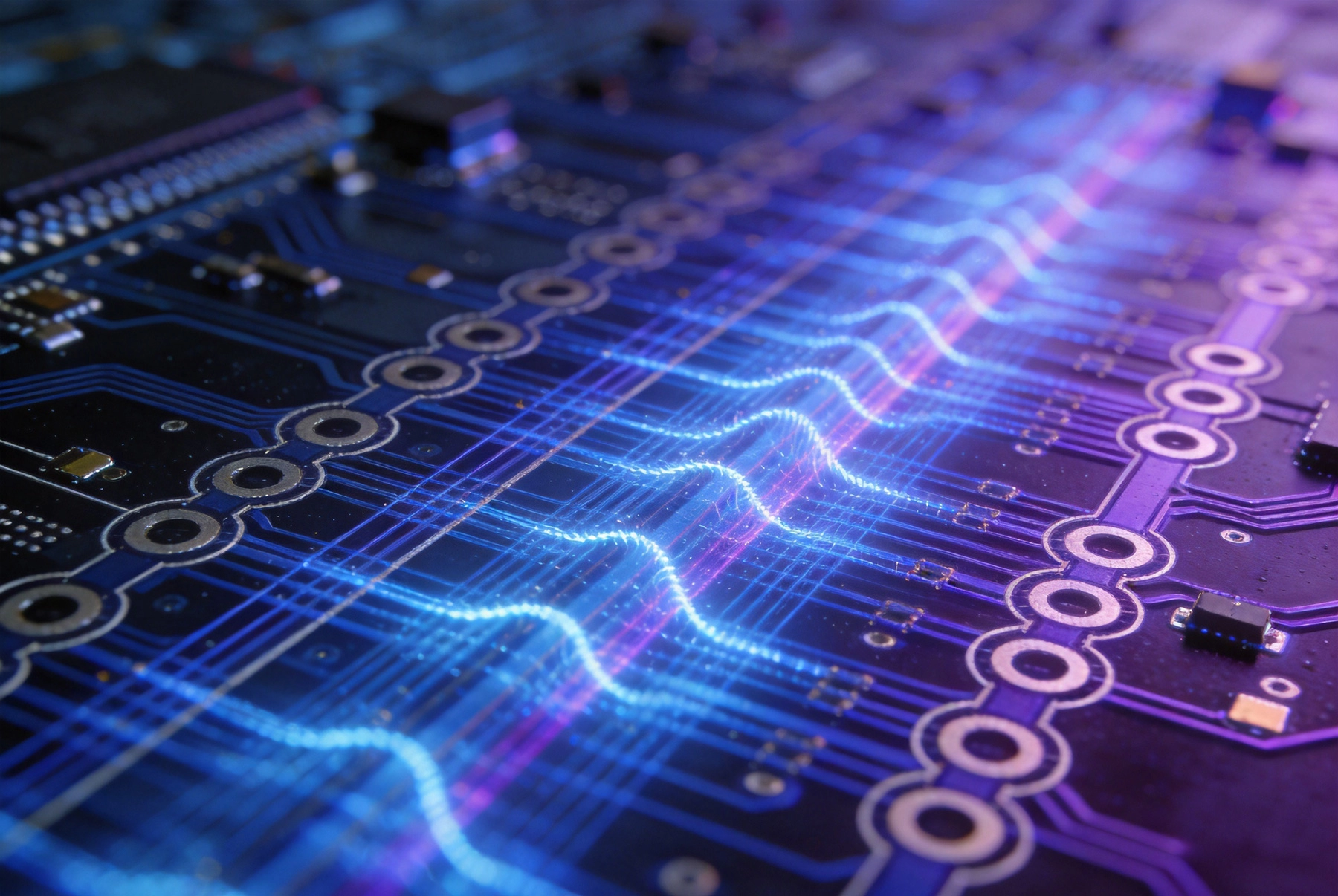
Crosstalk and Emi are both consequences of electromagnetic coupling — the transfer of energy from one conductor to another through their shared fields. The mechanism can be understood through two complementary models: capacitive (electric field) coupling and inductive (magnetic field) coupling. Both matter in PCB environments, but their relative importance shifts with frequency and geometry.
Capacitive coupling occurs when the electric field between two adjacent conductors induces a displacement current in the victim trace. In the context of a PCB, this happens between two traces running parallel to each other on the same layer or on adjacent layers with trace-to-trace overlap. The coupling coefficient — the fraction of the aggressor signal that appears on the victim — increases with the parallel run length, the frequency content of the signal, and the proximity of the two conductors. Reducing coupling means reducing any of these three factors: shorter parallel runs, lower frequency content at the coupling frequency, or greater physical separation.
Inductive coupling occurs when the changing magnetic field produced by current flow in the aggressor conductor induces a voltage in the victim through Faraday's law. This coupling is proportional to the mutual inductance between the two current loops — which depends on the loop areas formed by the signal and return path. The key insight is that the loop area, not just the trace width, determines inductive coupling. A trace with a return path that loops far away creates a larger effective antenna than the same trace with a solid reference plane directly beneath it.
A solid, continuous reference plane — almost always a Ground Plane — is the single most effective tool for managing electromagnetic coupling in PCB layouts. It does this in two ways simultaneously. Electrically, the reference plane shields the region above it from external fields and contains the fields of signals on the adjacent layer, preventing them from coupling into adjacent signal layers. Magnetically, a solid plane provides a low-inductance return path directly beneath the signal trace, minimizing the loop area and therefore the inductive coupling to neighboring circuits.
Slots, gaps, and splits in the reference plane are among the most common layout mistakes that cause Emi and crosstalk problems. A slot beneath a high-speed signal forces the Return Current to navigate around the slot, dramatically increasing the loop area for that segment of the trace. The magnetic field that results from this enlarged loop couples efficiently into adjacent signals. The fix is straightforward — do not route high-speed signals over slots or splits in the reference plane — but it requires the discipline to check plane integrity as part of every routing decision rather than treating plane fills as afterthoughts.
For mixed-signal designs where analog and digital circuits share a board, the reference plane strategy requires additional care. One approach is to use separate ground planes for analog and digital domains, connected at a single point — a technique called a split Ground Plane. Done correctly, this prevents digital switching noise from propagating into the analog section through the shared impedance of a single plane. Done incorrectly — for instance, by routing signals across the split — it creates worse problems than a solid shared plane would have. The key rule is that signals should never cross a plane split: any signal that transitions from the digital side to the analog side must do so through a component that straddles the boundary and provides a controlled crossing point.
The geometry of trace routing directly determines coupling strength. Parallel trace runs — the most common routing pattern on a PCB — are also the most couplable. The coupling factor between two parallel Microstrip traces increases approximately linearly with run length and decreases with the square of separation distance. This has a practical implication that designers often overlook: small increases in trace separation have a disproportionate effect on coupling. Doubling the spacing between two traces reduces crosstalk by roughly a factor of four. This is why the three-H rule — maintaining three trace-widths of separation between critical signals — is a useful starting heuristic, not an arbitrary number.
For the most sensitive signals, guard traces offer additional isolation. A guard trace is a grounded trace routed between an aggressor and a victim, providing a conductive barrier that shunts capacitive coupling current to ground before it reaches the victim. The guard trace must be grounded at regular intervals — typically at intervals of one-tenth of the wavelength of the highest frequency component in the signal — to be effective at high frequencies. At lower frequencies, longer guard trace segments can actually couple more noise to the victim by creating a secondary coupling path, so the guard trace approach is most effective for microwave and Rf Circuits where the wavelength is short enough to make frequent Grounding practical.
Differential pair routing is the standard approach for high-speed serial signals and clock distribution because it offers inherent noise rejection. By routing two signals in parallel with tight coupling to each other and to a shared reference plane, differential signaling converts the common-mode noise that couples equally into both traces into a differential voltage that the receiver rejects. The key requirement for effective differential routing is consistent electrical length — both traces must see the same total propagation delay from driver to receiver, accounting for the physical length difference and the velocity of propagation on the specific substrate. Length mismatches between the two legs of a differential pair create a skew that degrades the common-mode rejection at high frequencies.
Vias are discontinuities. At low frequencies, a via is just a vertical wire — its inductance and capacitance are small enough to be irrelevant. At high frequencies, every via introduces a parasitic inductance of roughly 0.3 to 1.0 nanohenry per millimeter of stub length, and a parasitic capacitance to the reference planes it passes through. These parasitics resonate with the trace impedance and the signal bandwidth, creating impedance mismatches that cause reflections and increase radiated emissions.
The stub length is often the controlling parameter. A via that passes completely through the board — a through via — leaves a stub of non-functional Transmission Line extending below the bottom layer. For signals with significant frequency content above a few gigahertz, this stub acts as a resonant antenna that can significantly increase EMI. The solution is to use back-drilled vias — mechanically drilled out to remove the non-functional stub portion — or to specify blind or buried vias that only extend as far as needed to reach the target layer. In high-speed backplanes and RF boards, back-drilling is standard practice precisely because the stub resonance would otherwise compromise Signal Integrity at the frequencies of interest.
Via-in-pad — routing vias directly into the component pad rather than offsetting them — improves thermal dissipation and reduces series inductance for power and ground connections, but it creates manufacturing challenges for signal vias because the plating and fill processes can introduce voids that affect reliability. For high-frequency signal routing, the practical recommendation is to keep vias off critical signal paths where possible and, where vias are unavoidable, to minimize their aspect ratio and to use back-drilling or blind via structures to control stub length.
The PCB dielectric properties — specifically the relative permittivity (Dk) and Dissipation Factor (Df) of the substrate — affect crosstalk and EMI in two competing ways. A higher Dk increases the effective capacitance between adjacent traces on the same layer, which increases capacitive coupling. But it also reduces the trace width required for a given impedance on a given layer thickness, which for a fixed pitch allows greater physical separation at the same impedance. The trade-off is not trivial, and the optimal choice depends on the frequency range, the geometry, and the relative importance of capacitive versus inductive coupling in the specific design.
Low-Dk, low-Df materials — Rogers RO4000 series, Panasonic Megtron, Isola I-tera — are increasingly used in high-frequency applications not because they reduce crosstalk directly, but because they offer more predictable impedance and lower loss at microwave frequencies. At frequencies above 5 GHz, the Dissipation Factor of standard Fr-4 (typically 0.02 to 0.035) introduces signal attenuation that degrades link budget and increases risetime, which indirectly exacerbates EMI by making rise times shorter and spectral content higher. Low-loss Materials address this at the cost of higher material pricing and, in some cases, reduced manufacturing yield due to different drilling and plating characteristics compared to Fr-4.
The layer stack sequence — which determines the distance between signal layers and reference planes — is as important as the material selection. A thin dielectric between the signal layer and its reference plane reduces loop inductance and makes the Transmission Line more immune to external fields. A thick separation between adjacent signal layers reduces capacitive coupling. Optimizing the stack-up means choosing dielectric thicknesses that match the requirements of each layer's signals, with the highest-frequency and most sensitive signals closest to the most solid reference planes.
When layout measures are insufficient to bring EMI within acceptable limits, Shielding becomes the last line of defense. Board-level Shielding — metal cans or conductive gaskets placed over sensitive RF or mixed-signal sections — attenuates radiated emissions by reflecting and absorbing electromagnetic energy. The effectiveness of a shield depends on the continuity of its enclosure: any gap or seam that is a significant fraction of a wavelength acts as a slot antenna, radiating more energy than an unshielded board would.
Conductive elastomer gaskets and fingers are used to maintain electrical continuity across shield seams and enclosure joints. The choice of gasket material and compression force must account for the operating environment — temperature extremes, vibration, and corrosion potential all affect gasket performance over the product lifecycle. For cost-sensitive applications where a full metal shield is impractical, conductive coatings applied to the plastic enclosure or board-level shielding films bonded to the PCB surface provide intermediate shielding effectiveness at lower cost.
Switching transients on the power distribution network (PDN) are a significant source of EMI in high-frequency digital circuits. When a digital output switches state, it draws a surge of current from the power supply through the PDN. The inductance of the PDN — including the bypass capacitors, the power and ground plane structures, and the package leads — causes a voltage drop at the device pin during the switching transient. This transient voltage drop appears as noise on the local power rail and couples into adjacent signal traces through the power and ground connections shared between them.
Proper decoupling — placing capacitors as close as possible to the power pins of each IC, with short wide traces or plane connections to minimize series inductance — controls the impedance of the PDN at the frequencies where switching transients occur. For devices with risetimes below 500 picoseconds, conventional discrete decoupling capacitors begin to lose effectiveness because their own ESL (Equivalent Series Inductance) becomes the limiting factor. In these cases, embedded capacitance — placing dedicated power and ground planes separated by a very thin dielectric — provides a lower-inductance decoupling structure that is effective up to substantially higher frequencies.
PCB-level Electromagnetic Simulation — using 3D full-wave solvers such as HFSS or CST to model the complete board structure — has become increasingly accessible as computational costs have fallen. For designs operating above 1 GHz or where Signal Integrity margins are tight, a simulation-based signal integrity analysis before layout finalization can identify crosstalk and EMI risks that are difficult or impossible to detect with layout rules alone. The key deliverables from such an analysis include far-field radiation plots that predict the EMI signature of the board, S-parameter extraction of critical nets for time-domain analysis, and identification of resonance modes in the board cavity that could amplify coupling between specific trace pairs.
Measurement with a vector network analyzer (Vna) and near-field probes provides validation that simulation models are accurate and that the manufactured board behaves as predicted. Near-field scanning — moving a magnetic or electric field probe over the board surface to map field intensity — is particularly useful for identifying EMI hot spots on a prototype before committing to production. The workflow that combines simulation prediction with prototype measurement — iterating the model until the simulation and measurement agree — builds confidence that the design will meet its electromagnetic compatibility requirements in production.
Experienced designers encode their crosstalk and EMI management knowledge into the PCB design rules that govern their layouts. A comprehensive rule set for high-frequency designs typically includes maximum parallel run lengths between critical signals, minimum spacing rules differentiated by signal type (clock, data, power, RF), via stub length limits enforced by the fabrication specification, reference plane integrity checks that flag routing over slots or splits, and differential pair length mismatch tolerances that account for the specific data rate and acceptable skew budget.
These rules should be understood not as restrictions but as the distillation of electromagnetic theory into actionable constraints. When a designer understands why the three-H rule reduces crosstalk by approximately 75 percent compared to a one-H separation, they can make intelligent trade-offs when geometry demands it — accepting the crosstalk penalty in a constrained area while compensating through other means, such as shorter parallel run lengths on adjacent sections of the route.
Managing crosstalk and EMI in dense High-frequency Pcb layouts is fundamentally an electromagnetic design problem that manifests as a layout problem. The coupling mechanisms — capacitive and inductive — are well understood physics, and the mitigation techniques — reference plane integrity, trace separation, differential routing, via stub control, proper decoupling — are well-established engineering practice. What distinguishes successful high-frequency designs is the discipline to apply these principles consistently throughout the layout process, validated against simulation and measurement as the design matures. In an era of ever-increasing signal speeds and ever-denser layouts, this discipline is not optional — it is the difference between a product that meets its specifications and one that fails unexpectedly in the field.
Essential High Frequency PCB Knowledge for Hardware Engineers and DesignersMay/29/2026
High Frequency PCB Knowledge: How to Minimize Insertion Loss and ReflectionJuly/21/2026
Essential High Frequency PCB Knowledge for Hardware Engineers and DesignersJune/15/2026
Key High Frequency PCB Knowledge for Successful RF Circuit DesignSeptember/07/2026

High Frequency PCB Knowledge: The Difference Between High-Speed and High-FrequencySeptember/17/2026
Advanced High Frequency PCB Knowledge: Using Simulation Tools for Better ResultsSeptember/29/2026
High Frequency PCB Knowledge: Best Practices for Grounding and ShieldingOctober/12/2026
The Engineer's Guide to High Frequency PCB Knowledge and Stack-up DesignJuly/31/2026