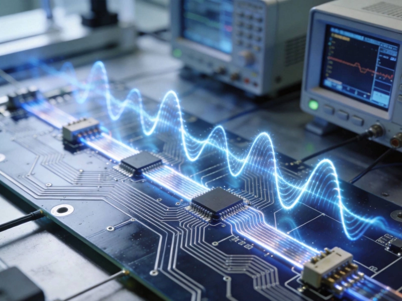
high frequency PCB prototypes represent a significant investment in both time and resources. After weeks or months of design effort and manufacturing lead times, receiving the first prototype brings anticipation and anxiety. Will it work as designed? Will it meet the performance specifications required for the intended application? For high frequency applications—ranging from 5g Telecommunications and radar systems to high-speed digital interfaces and Aerospace Electronics—these questions become critical because performance margins are often narrow and failure consequences are severe.
Testing and validation represent the crucial bridge between design intent and verified performance. A comprehensive testing strategy ensures that high frequency PCB prototypes meet specifications, identifies design or manufacturing issues early, and provides confidence before committing to volume production. This article explores the complete testing and validation process for high frequency PCBs, from basic continuity checks through sophisticated RF measurements, helping you develop a validation approach appropriate for your application's requirements.

The Testing Hierarchy for High Frequency PCBs
Progressive Validation Approach
Effective testing follows a structured progression from basic to sophisticated measurements:
- Structural verification – Confirming physical construction and electrical connectivity
- DC parameter testing – Verifying basic electrical characteristics
- AC performance validation – Signal Integrity and frequency response
- RF parameter measurement – High-frequency performance characteristics
- Functional testing – System-level operation under realistic conditions
Each level builds on previous testing, with failures at early stages saving time by preventing unnecessary investment in more complex measurements.
Test Planning and Preparation
Before testing begins, establish clear objectives:
- Specification review – Documenting required performance parameters
- Test procedure development – Detailed step-by-step test plans
- Equipment verification – Ensuring test equipment calibration and capability
- Test fixture design – Creating appropriate connections and interfaces
- Success criteria definition – Establishing pass/fail thresholds
Structural and Connectivity Testing
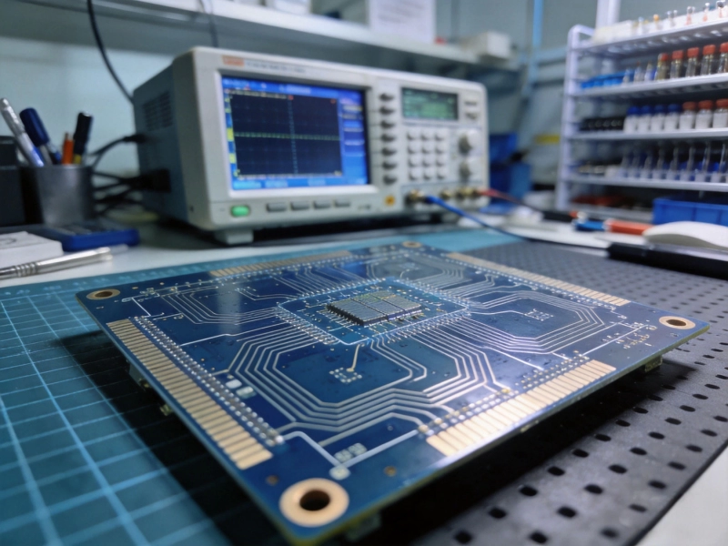
Visual and Microscopic Inspection
Begin with thorough physical examination:
- Visual inspection – Checking for obvious manufacturing defects
- Microscopic examination – Verifying fine features and solder joints
- Dimensional verification – Confirming critical dimensions
- Layer stack-up validation – Cross-sectional analysis for multilayer boards
For high frequency boards, pay special attention to Transmission Line geometry, via structures, and Ground Plane integrity.
Electrical Continuity and Isolation
Basic electrical testing confirms proper construction:
- Continuity testing – Verifying all intended connections exist
- Isolation testing – Confirming no unintended shorts
- High-potential testing – Verifying insulation integrity at elevated voltages
- Resistance measurement – Checking for excessive resistance in power and ground paths
These tests identify catastrophic manufacturing failures before proceeding to more complex measurements.
DC Parameter Validation
Resistance and Impedance Measurement
DC electrical characteristics provide insight into design implementation:
- Trace resistance – Measuring actual resistance vs. calculated values
- Power supply distribution – Verifying IR drop and voltage levels
- Ground Plane continuity – Ensuring low-impedance ground connections
- Component values – Verifying passive component values and tolerances
Leakage and Insulation Testing
High voltage and leakage tests verify isolation:
- Insulation resistance – Measuring resistance between isolated conductors
- Dielectric withstanding voltage – Hi-pot testing for insulation strength
- Leakage current measurement – Checking for unintended current paths
Signal Integrity Testing
Time Domain Analysis
Time domain measurements evaluate signal quality in the time domain:
- Waveform analysis – Examining signal rise time, fall time, and overshoot
- Eye diagram generation – Evaluating Signal Integrity through eye patterns
- Jitter measurement – Quantifying timing jitter and phase noise
- Skew measurement
– Verifying timing alignment between multiple signals
Time domain reflectometry (TDR) provides critical insight into impedance discontinuities and Transmission Line quality.
Impedance Measurement
Controlled Impedance is critical for high frequency performance:
- Characteristic Impedance – Measuring actual vs. target impedance (typically 50Ω, 75Ω, or 100Ω)
- Time domain reflectometry – Identifying impedance discontinuities and reflections
- Frequency domain impedance – Measuring impedance across frequency range
- Differential impedance – Verifying differential pair characteristics
Target impedance tolerance varies by application but typically requires ±10% or better for high-speed digital and RF applications.
Loss measurements characterize signal degradation:
- Insertion Loss – Measuring signal attenuation through the transmission path
- Return loss – Quantifying reflected signal due to impedance mismatches
- VSWR (Voltage Standing Wave Ratio) – Alternative return loss measure commonly used in RF
- S-parameters – Complete scattering parameter characterization
RF and Microwave Testing
S-Parameter Measurement
S-parameters provide comprehensive RF characterization:
- S11 – Return loss – Input reflection coefficient
- S21 – Insertion loss – Forward transmission
- S12 – Reverse transmission – Isolation and reverse transmission
- S22 – Output return loss – Output reflection coefficient
Vector network analyzers (VNAs) measure S-parameters across frequency ranges from kHz to 110 GHz or higher.
Frequency Response Analysis
Frequency domain measurements reveal frequency-dependent behavior:
- Gain/flatness – Measuring amplification variation across frequency
- Bandwidth measurement – Determining useful frequency range
- Group delay – Measuring phase linearity and delay characteristics
- Phase response – Analyzing phase characteristics vs. frequency
Noise Figure and Sensitivity
For receiver and low-noise applications:
- Noise figure measurement – Quantifying signal-to-noise degradation
- Noise temperature – Alternative noise figure measure
- Sensitivity measurement – Determining minimum detectable signal
- Dynamic range – Measuring usable signal range
Emi and Emc Testing
Emissions Testing
Electromagnetic Compatibility requires emissions validation:
- Conducted emissions – Measuring noise on power and signal lines
- Radiated emissions – Measuring electromagnetic radiation
- Harmonic analysis – Identifying harmonic content
- Spurious emissions – Detecting unintended signal generation
Immunity and Susceptibility
Robustness to external interference:
- Conducted immunity – Testing resistance to power line disturbances
- Radiated immunity – Measuring resistance to external fields
- Electrostatic discharge (ESD) – Verifying ESD robustness
- Electrical fast transient (EFT) – Testing transient immunity
Environmental and Reliability Testing
Temperature Testing
High frequency performance varies with temperature:
- Cold temperature operation – Verifying performance at minimum specified temperature
- Hot temperature operation – Confirming operation at maximum specified temperature
- Thermal cycling – Testing reliability through temperature transitions
- Thermal shock – Rapid temperature change survival
Vibration and Mechanical Stress
Mechanical reliability testing:
- Vibration testing – Simulating transportation and operational vibration
- Mechanical shock – Testing resistance to mechanical impacts
- Bend testing – For flexible circuits or applications with flexing
- Humidity testing – Verifying performance in high-humidity environments
Test Equipment and Instrumentation
Essential Measurement Equipment
High frequency testing requires specialized instruments:
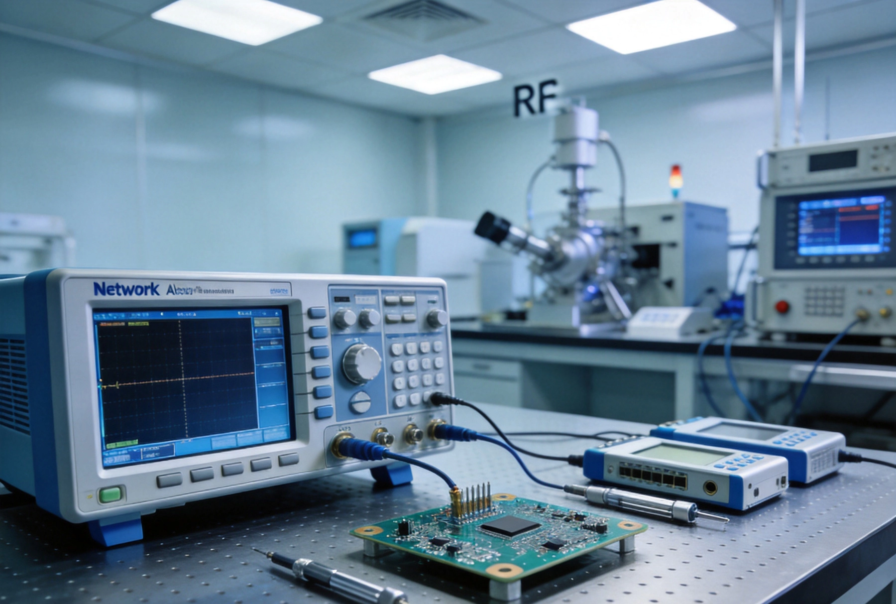
- Vector Network Analyzer (VNA) – S-parameter and impedance measurements
- Time Domain Reflectometer (TDR) – Impedance and discontinuity analysis
- Oscilloscope – Time domain waveform and eye diagram analysis
- Spectrum analyzer – Frequency domain and emissions measurements
- Signal generator – Providing test signals for characterization
Calibration and Reference Standards
Accurate measurements require proper calibration:
- Calibration verification – Confirming instrument accuracy
- Reference standards – Using known reference materials for validation
- Measurement uncertainty – Understanding and accounting for measurement error
- Traceability – Ensuring measurements trace to national standards
Test Fixture and Interface Design
Probe Selection and Contact Methods
Accurate measurements depend on proper connections:
- High-frequency probes – Minimizing probe loading and parasitic effects
- Ground spring contacts – Ensuring low-inductance ground connections
- Probe positioning – Minimizing lead length and loop area
- Contact force – Ensuring reliable low-resistance contact
Test Fixture Design
Custom fixtures enable repeatable measurements:
- RF connectors – 2.4mm, 2.92mm, 3.5mm, SMA, or other appropriate connectors
- Transmission line design – Maintaining Controlled Impedance in fixtures
- Minimizing discontinuities – Smooth transitions from fixture to DUT
- Ground plane integrity – Ensuring proper ground reference
Interpreting Test Results
Pass/Fail Criteria
Clear criteria enable objective evaluation:
- Specification comparison – Direct comparison to design requirements
- Margin analysis – Quantifying headroom beyond requirements
- Trend analysis – Identifying performance patterns
- Correlation with simulation – Comparing measurements to design predictions
Root Cause Analysis
When tests fail, systematic investigation identifies causes:
- Design verification – Checking design calculations and assumptions
- Manufacturing inspection – Examining physical construction for defects
- Material verification – Confirming material properties match specifications
- Measurement validation – Verifying test setup accuracy
Documentation and Reporting
Test Report Contents
Comprehensive test reports document findings:
- Test procedures – Detailed methodology used
- Equipment information – Instrument models and calibration status
- Test results – Raw data and calculated values
- Graphs and charts – Visual presentation of measurement data
- Conclusions and recommendations – Assessment and improvement suggestions
Traceability and Version Control
Maintaining test history supports continuous improvement:
- Version identification – Linking results to specific board revisions
- Configuration tracking – Documenting test configurations
- Baseline establishment – Creating reference data for comparison
- Change tracking – Correlating design changes with test results
Common Testing Issues and Solutions
Measurement Artifact Elimination
Many apparent issues are actually measurement artifacts:
- Probe loading – Using low-capacitance probes for minimal loading
- Ground bounce – Implementing proper Grounding techniques
- Fixture resonances – Designing fixtures with adequate bandwidth
- Cable effects – Using high-quality cables and proper terminations
Design vs. Measurement Discrepancies
When measurements don't match simulations:
- Model verification – Checking simulation model accuracy
- Material parameter verification – Confirming Dielectric Constant and loss tangent
- Manufacturing tolerance – Accounting for dimensional variations
- Environmental factors – Considering temperature and humidity effects
Best Practices for High Frequency Testing
Test Strategy Development
Develop testing strategies aligned with application requirements:
- Risk-based testing – Focusing on critical performance parameters
- Cost-effective approach – Balancing test thoroughness with resources
- Iterative testing – Testing throughout design iterations
- Collaborative approach – Involving design, manufacturing, and test teams
Continuous Improvement
Use test data for design enhancement:
- Design refinement – Applying test insights to design improvements
- Process optimization – Adjusting manufacturing based on test results
- Test method improvement – Enhancing testing techniques for better accuracy
- Knowledge base development – Building institutional test expertise
Conclusion
Testing and validation represent the critical final step in high frequency pcb development, confirming that design intent translates into actual performance. A comprehensive testing approach—progressing from basic structural verification through sophisticated RF measurements—ensures that prototypes meet specifications and provides confidence before committing to production.
high frequency pcb testing demands specialized equipment, careful technique, and deep understanding of both the device under test and measurement system limitations. When executed properly, testing not only validates performance but also provides insights that can drive design improvements, enhance reliability, and reduce risk throughout the product lifecycle.
As high frequency applications continue pushing toward higher speeds, wider bandwidths, and more complex integration, the role of comprehensive testing becomes increasingly important. Companies that invest in thorough validation processes develop products with superior performance, higher reliability, and faster time-to-market—critical advantages in competitive high-frequency electronics markets.
Our testing laboratory offers comprehensive validation for High Frequency Pcb prototypes, from impedance measurement to full S-parameter characterization. With state-of-the-art equipment and experienced engineers, we provide the confidence you need before committing to production. Contact us to discuss your testing requirements.
Frequently Asked Questions
What test equipment is essential for high frequency PCB validation?
Essential equipment includes a vector network analyzer (VNA) for S-parameter measurements, a time domain reflectometer (TDR) for impedance analysis, a high-bandwidth oscilloscope for time domain analysis, and a spectrum analyzer for emissions and frequency domain measurements.
How accurate must impedance measurements be for high frequency designs?
Typical impedance tolerance requirements range from ±5% to ±10% for most high-speed digital and RF applications, though some demanding applications require ±2% or better. Measurement accuracy should be at least twice as precise as the required tolerance.
When should environmental testing be performed on high frequency PCBs?
Basic functional testing should occur first, followed by environmental testing for boards that must operate in extreme conditions. Thermal testing is particularly important for high frequency designs because dielectric properties and material dimensions vary with temperature.
How do I distinguish between actual performance issues and measurement artifacts?Systematic troubleshooting helps: verify test equipment calibration, check fixture and connections, use different measurement techniques to cross-validate, and compare results with simulation predictions. Measurement artifacts typically show inconsistencies across different test methods.
What are the most common failures in high frequency PCB prototype testing?
Common issues include impedance mismatch causing reflections, excessive insertion loss, poor return loss due to transitions, inadequate isolation causing crosstalk, and Emi/Emc problems. Most of these can be traced to design oversights, manufacturing variations, or material property deviations.