
Your 5g Base Station operates flawlessly in the lab. Then production units start arriving with intermittent connectivity issues, phantom signals, and mysterious data errors. What changed? The components are identical. The designs match. The difference lives in the invisible details of assembly—and Signal Integrity paid the price.
high frequency PCB assembly presents challenges that disappear at lower frequencies. What works perfectly for 100MHz digital logic fails catastrophically at 5GHz or 77GHz Automotive Radar. The gap between "good enough" and "actually working" narrows dramatically as frequencies climb. Understanding how assembly processes affect Signal Integrity isn't optional for RF engineers—it's survival.
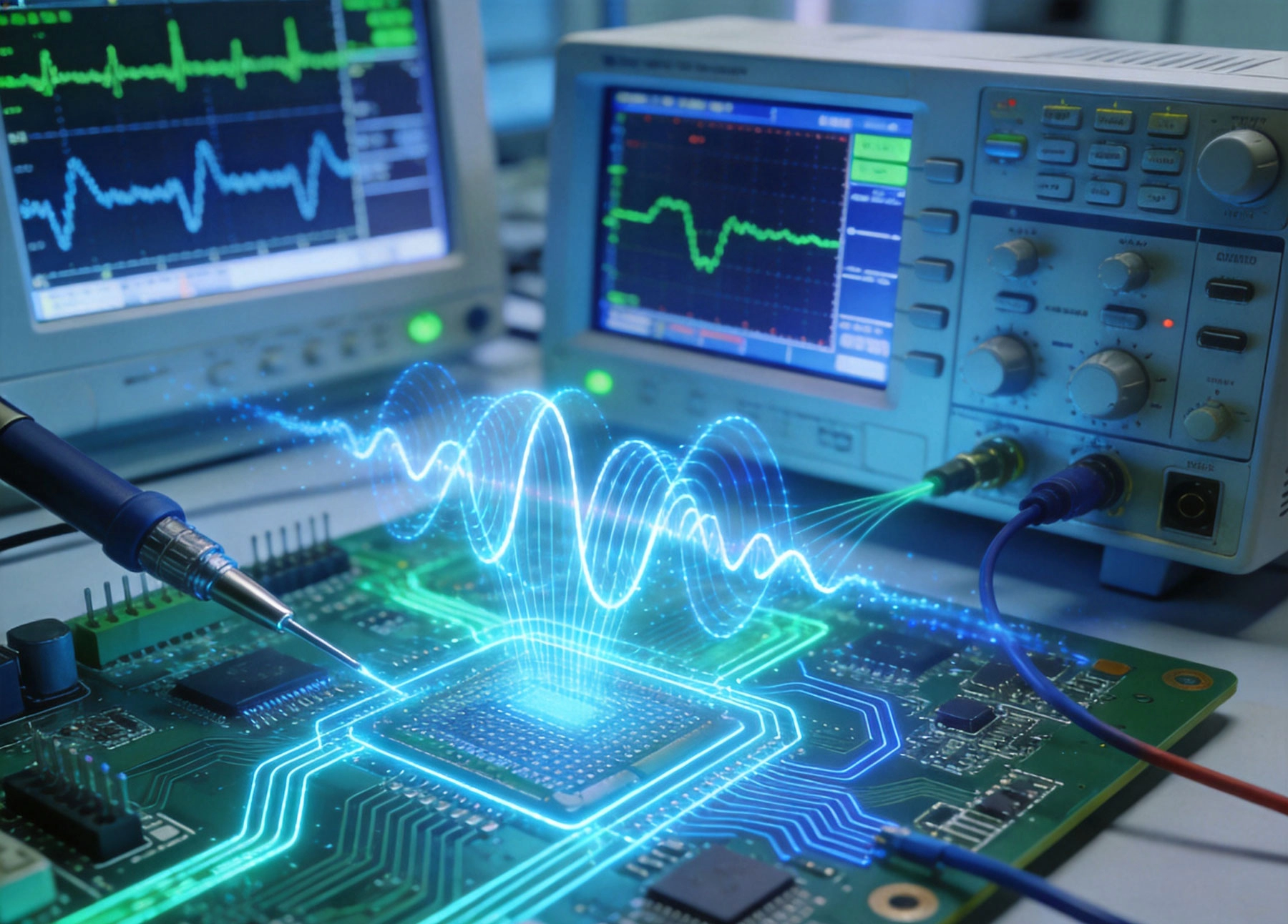
At low frequencies, electrons flow like water through a pipe. At high frequencies, they slosh like waves in a tank. This shift in behavior transforms PCB design and assembly from geometric layout exercises into electromagnetic engineering problems.
At DC, current distributes uniformly across conductor cross-section. At RF frequencies, current crowds toward conductor surfaces—a phenomenon called Skin Effect. At 10GHz, skin depth in copper is roughly 0.65μm. This means only the outer micron of your trace conducts.
Surface roughness, plating irregularities, and contamination that would be invisible at low frequencies become significant loss mechanisms at RF. Assembly processes that roughen surfaces or introduce plating variations degrade signal transmission measurably.
Signal propagation time across a PCB becomes significant relative to signal rise time at high frequencies. A 1ns rise time signal traverses 15cm before completing its transition. If this distance approaches your board dimensions, you must account for propagation delay in your timing budget.
More critically, mismatched impedance causes reflections that distort signal edges and create standing waves. These effects are negligible at 100MHz but devastating at 10GHz. Assembly variations that shift trace dimensions by micrometers can move impedance enough to cause failures.
Pcb Substrate Materials absorb energy differently at various frequencies. Loss tangent (Df) quantifies this absorption. Standard Fr-4 has Df around 0.02 at 1GHz—acceptable for digital work. At 10GHz, Fr-4 losses increase substantially, making specialized materials necessary.
Assembly processes can affect effective Dielectric Constant through moisture absorption, material stress, or thermal damage. Understanding these mechanisms helps you prevent performance degradation.
Successful high frequency assembly starts with design decisions that enable manufacturing success.
Controlled Impedance traces require precise dimensional control throughout manufacturing. Target impedance tolerances of ±10% (acceptable for digital work) tighten to ±5% or ±3% for RF applications. Achieving this precision requires traces that are:
Work with your manufacturer early to establish achievable tolerances for your stack-up configuration.
Pads for high frequency components must balance solderability against parasitics. Large pads provide manufacturing margin for reliable soldering but create capacitive loading that affects impedance. The pad dimensions specified on datasheets represent starting points—optimization for your specific application may be necessary.
Via structures present particular challenges. Through-hole vias introduce impedance discontinuities and parasitic inductance. For critical RF paths, consider:
High frequency signals return through the path of least impedance—not necessarily the shortest physical path. This means return currents flow beneath signal traces on reference planes. Gaps, slots, or Via Stitching breaks in reference planes redirect return currents, creating common-mode noise and increasing crosstalk.
Assembly designers must maintain continuous reference planes under high frequency traces. Via Stitching at 1/10 wavelength intervals keeps return currents close to signal paths and prevents mode conversion.
High Frequency Materials affect how boards behave during manufacturing processes.
Materials designed for RF and microwave applications include:
Each material has different thermal coefficients of expansion (TCE), moisture absorption, and processing requirements. Match material selection to your manufacturing partner's capabilities and your application requirements.
Multi-layer boards stack cores and prepreg layers. Prepreg flows during lamination, changing thickness and potentially affecting Controlled Impedance traces on adjacent layers. For tight Impedance Control, specify prepreg types and thicknesses that your manufacturer stocks and processes consistently.
Some manufacturers offer laser-etched impedance features where traces are adjusted after lamination to hit exact impedance targets. This technique costs more but achieves tolerances impossible with standard process variation.
Surface finish affects high frequency performance through:
For frequencies above 10GHz, ENIG (electroless nickel immersion gold) may introduce losses due to nickel diffusion layer properties. Alternative finishes like EPIG (electroless palladium immersion gold) or silver finishes may perform better for ultra-high frequency applications.
Manufacturing processes introduce variations that affect high frequency performance in ways invisible to standard testing.
Solder volume variation affects Component Placement height, which shifts impedance in Transmission Line structures. For controlled impedance lines, specify solder paste volumes and print processes that achieve consistent deposit heights.
Stencil design becomes critical. Aperture shape, aspect ratio, and wall quality affect print volume. Fine-pitch components may require electroformed stencils with polished walls for consistent release.
Thermal profiles affect High Frequency Materials differently than standard FR-4. Some RF laminates are rated for specific peak temperatures and dwell times. Exceeding these limits causes delamination, voiding, or changes to dielectric properties.
Profile optimization for mixed-material boards—combining Rf Materials with standard FR-4—requires balancing thermal requirements across all components. RF areas may need localized protection or special profiling to prevent thermal damage.
High frequency components often use controlled impedance launches—ground-signal-ground pin configurations where position and orientation affect RF performance. Placement accuracy of ±50μm or better may be necessary to maintain consistent impedance at component interfaces.
Verify that your assembly partner's placement equipment achieves the accuracy your design requires. Request capability studies for critical components, especially for BGA or QFN packages with RF pin arrays.
Maintaining controlled impedance through assembly requires attention to factors that affect effective trace dimensions and dielectric properties.
Etching, plating, and solder mask application all affect final trace dimensions. Each process step may shift effective trace width by ±10μm or more. For 200μm wide traces at 50Ω, this variation is ±5%—acceptable. For 100μm traces, the same variation becomes ±10%—potentially outside tolerance.
Design rules must account for cumulative manufacturing variation. Specify minimum trace widths that provide margin against process capability limits.
Effective dielectric constant depends on substrate material, thickness, and any coverings (solder mask, Conformal Coating). Assembly processes that introduce moisture, thermal stress, or chemical contamination can shift effective Dk.
Control processes that affect board properties after impedance testing: solder mask application changes effective Dk slightly. Conformal Coating affects covered traces. If your impedance-critical paths need coating, test impedance after coating rather than before.
Pcb Materials have temperature coefficients of dielectric constant (TCDk). At constant frequency, Dk changes with temperature, which shifts impedance. For applications with wide temperature ranges—automotive under-hood, industrial environments—temperature compensation may be necessary.
Assembly processes that subject boards to elevated temperatures—multiple reflow cycles, hot air leveling, accelerated thermal aging—can permanently shift material properties. Document thermal history and re-test impedance after any high-temperature processing.
Standard electrical testing doesn't catch high frequency issues. Specialized approaches are necessary.
Tdr testing sends fast rise-time pulses down Transmission Lines and measures reflections. Discontinuities appear as impedance steps that pinpoint location. Tdr can identify:
Most high-frequency test equipment includes TDR capability. Specify TDR testing for impedance-critical nets.
Vna measurements quantify S-parameters—scattering parameters—that fully characterize RF performance. Key measurements include:
Vna testing requires calibration standards and skilled interpretation. Not all assembly houses have VNA capability—verify before production.
High frequency testing supplements but doesn't replace standard continuity testing. High frequency opens—poor joints invisible to resistance measurement—cause RF failures. High frequency shorts—contact between adjacent traces at RF—create coupling that corrupts signals.
Specify both DC continuity testing and Rf Testing for complete coverage.
Understanding typical failure modes helps prevent them.
Marginal solder joints may pass DC continuity testing but fail under RF excitation. Vibration, thermal cycling, or mechanical stress can develop cracks that grow over time. For mission-critical applications, vibration testing and thermal cycling with Rf Testing after stress reveals marginal joints.
Plated-through holes, component pads, and routing transitions all create impedance discontinuities. Individual discontinuities may be tolerable. Cascaded discontinuities—multiple imperfect transitions in sequence—cause accumulated reflections that degrade signal quality.
Use Em Simulation tools to model your routing and identify problematic cascade effects before manufacturing.
High frequency coupling between adjacent traces or components causes crosstalk. Assembly variations that change trace spacing—solder mask bridging, misaligned layers, component shift—increase coupling beyond designed levels.
Specify minimum trace spacing for controlled impedance lines and verify spacing after assembly using cross-sectional analysis or X-ray Inspection.
Consistency separates acceptable high frequency assembly from excellent high frequency assembly.
Track critical parameters across production:
Control charts showing parameters within statistical limits provide confidence that production boards match qualification samples.
Material lot variations—prepreg Dk batch differences, laminate thickness variations—affect impedance. Lot traceability enables correlation of assembly performance to material lots, identifying problematic lots before production.
Request material traceability documentation from your manufacturer and maintain records that enable field failure investigation.
Every new board design, material change, or significant process change requires first article inspection. Include in your inspection:
First article approval should be a prerequisite for production release.
Not all assembly houses handle high frequency work equally well. Qualification requirements go beyond standard ISO certifications.
Ask potential suppliers for:
Request sample boards demonstrating their capability before committing to production.
High frequency materials require specialized procurement and handling. Suppliers with established relationships with Rogers, Isola, or other high-frequency laminate manufacturers get better pricing, faster delivery, and fresher material (important for moisture-sensitive materials).
Verify your assembly partner stocks the specific materials your design requires or can procure them reliably.
The best assembly partners engage during design rather than just production. They review controlled impedance requirements, suggest manufacturable stack-ups, and identify potential problems before manufacturing begins.
Price differences between suppliers often reflect design support quality. The lowest-cost supplier may be most expensive overall when design issues cause production problems.
High frequency assembly continues evolving to meet demanding applications.
Automotive Radar at 77GHz and upcoming 120GHz sensors push frequency even higher. At these wavelengths, traditional PCB approaches reach fundamental limits. Technologies like antenna-in-package and Advanced Substrate Materials enable continued progress.
Embedding passive components within PCB layers eliminates surface-mount parasitics. For high frequency applications, embedded resistors and capacitors can improve performance by removing discrete component discontinuities.
Current embedded component technology is mature for digital applications but still developing for high frequency. Monitor this space for future opportunities.
Research continues on Ultra-low Loss Materials, integrated antenna structures, and substrates with engineered dielectric properties. These advances will enable new applications while making existing ones less expensive.
Signal integrity at high frequency depends on manufacturing precision that standard electronics assembly doesn't require. The invisible variations that disappear at lower frequencies—micrometer trace differences, slight impedance shifts, minor discontinuities—become critical failure mechanisms as frequencies climb.
Success requires viewing assembly as part of the electromagnetic design, not just physical implementation. Design rules must account for manufacturing capability. Process control must maintain the consistency that high frequency performance demands. Testing must verify what matters, not just what's convenient.
The investment in high-frequency-capable assembly partners, materials, and testing pays through products that work—not just in the lab, but in production, over temperature, over time, and in the field.
As wireless applications continue expanding into higher frequency bands, signal integrity during assembly becomes ever more critical. Building this capability now prepares your organization for the demanding applications ahead.
Rules of thumb suggest special attention above 1GHz, with full controlled impedance requirements above 3GHz. However, fast digital signals with sub-nanosecond edges also create high-frequency effects on PCB traces. Always analyze your signal's effective frequency content when deciding on requirements.
Controlled impedance testing using TDR typically costs $50 to $200 per test coupon, with coupons typically included on each production panel. VNA testing is more expensive but provides comprehensive characterization. Budget $0.05 to $0.20 per square inch for impedance testing depending on complexity.
FR-4 can work for frequencies up to approximately 3-5GHz depending on loss requirements. Above that, FR-4 losses become prohibitive and specialized materials become necessary. Consult your manufacturer about stack-up options for your specific frequency range.
Failure to account for manufacturing variation in impedance design. Designers specifying theoretical trace widths without accounting for process capability often find production impedance outside tolerance. Always validate designs against actual manufacturing capabilities.
Request process capability studies showing Impedance Control statistics, cross-sectional documentation of their structures, and sample boards demonstrating their capability. If they can't provide this documentation, they may not have the experience or process control high frequency work requires.
At minimum, specify TDR testing on impedance-critical traces with defined tolerance limits. For applications above 10GHz, request VNA S-parameter testing and cross-sectional analysis. Always include continuity and isolation testing as well.
This article is intended for informational purposes. Consult with qualified RF engineers and experienced high-frequency Pcb Assembly manufacturers for specific application requirements.

Why Component Placement is Critical in High Frequency PCB AssemblyJune/25/2026
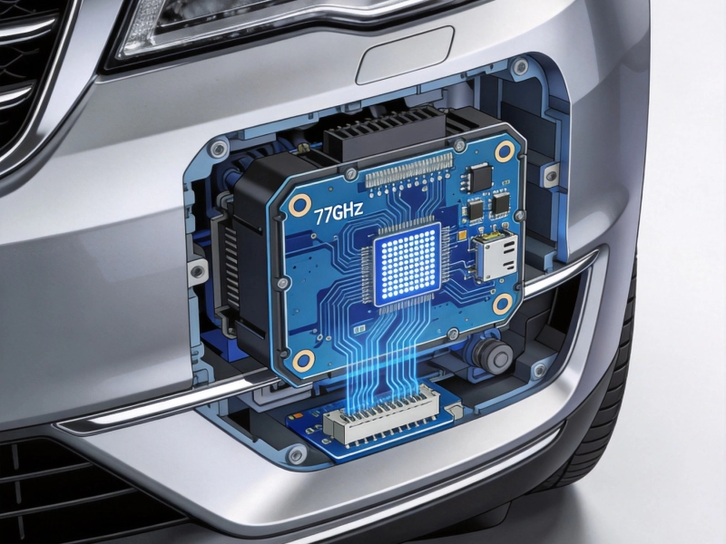
High Frequency PCB Assembly for Automotive Radar: Precision and ReliabilitySeptember/21/2026
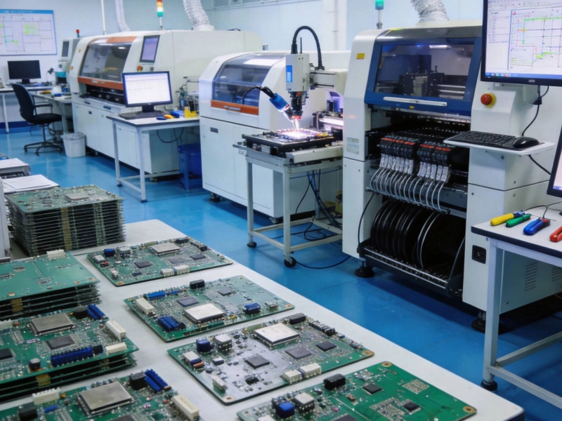
The Challenges of High Frequency PCB Assembly: Handling Sensitive ComponentsMay/29/2026

How to Select a Turnkey High Frequency PCB Assembly PartnerAugust/06/2026
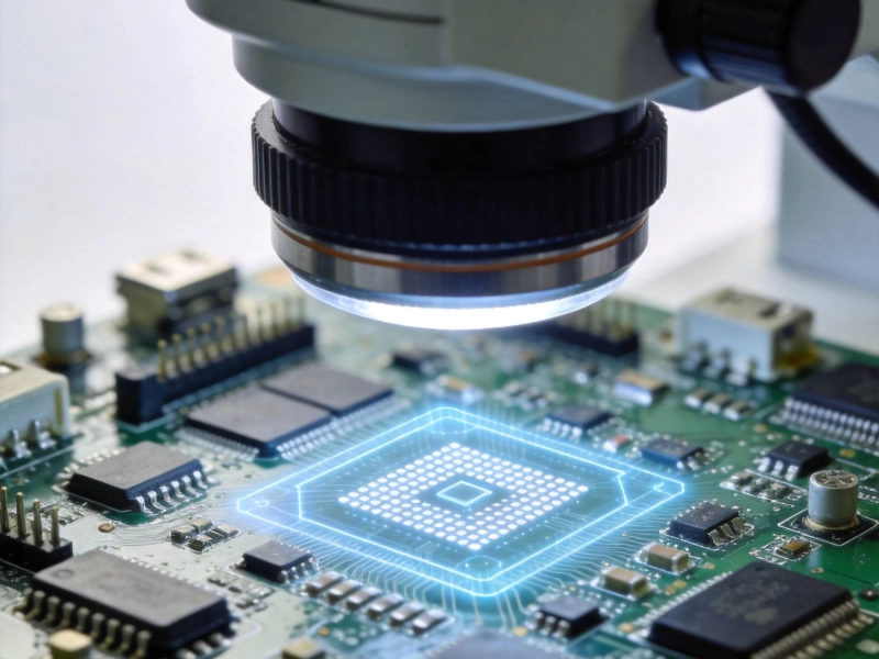
Avoiding Soldering Defects in High Frequency PCB Assembly for RF ApplicationsSeptember/11/2026
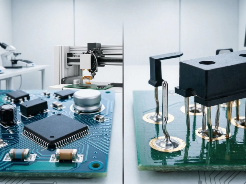
SMT vs. THT: Assembly Techniques for High Frequency PCBsJuly/03/2026
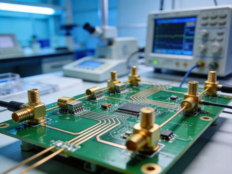
High Frequency PCB Assembly Best Practices for 5G and RF ModulesJune/08/2026
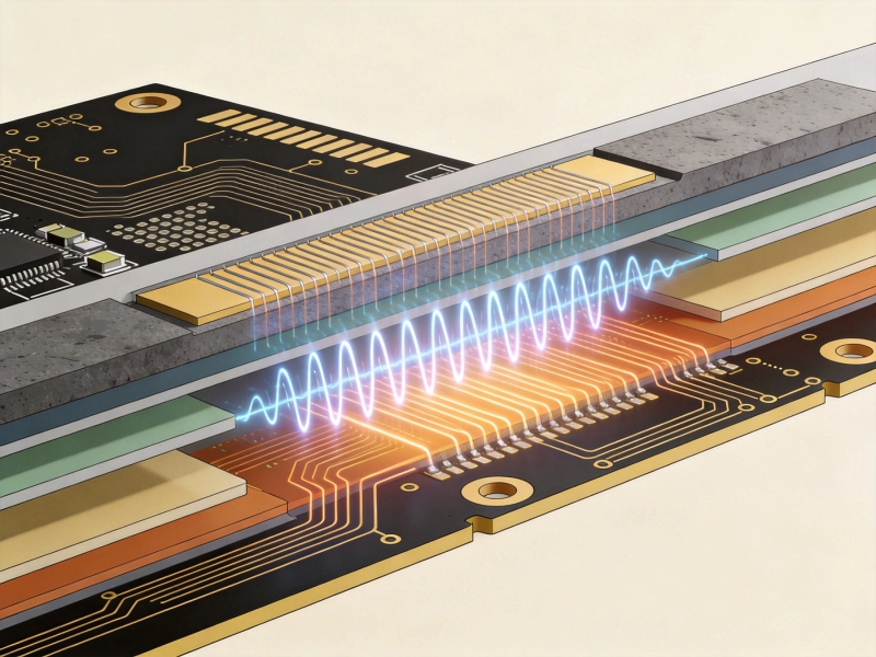
How Dielectric Constant (Dk) and Loss Factor (Df) Affect High Frequency PCB MaterialsJuly/20/2026