Open Nav
6g Research ain't just about dreaming up faster wireless speeds - it's about solving real engineering challenges that push existing technology to its limits. When researchers are working with frequencies potentially reaching hundreds of gigahertz, the PCBs that support their experiments gotta be something special. That's where we come in.
We've been pushing our High Frequency Pcb capabilities further and further, developing fabrication techniques and material expertise that make 6g Research possible. In this article, we'll share what we've learned, what we can do now, and how our capabilities are helping researchers push the boundaries of wireless technology. No marketing fluff - just technical capabilities you can actually use.

6G is projected to operate in frequency ranges that 5G barely touches - potentially up to 300 GHz and beyond. At these frequencies, everything about PCB design and fabrication becomes critical. Signal losses that were tolerable at 5G frequencies become devastating at 6G frequencies. Impedance tolerances that worked before now need to be much tighter.
Key PCB challenges for 6G research:
We recognized early that supporting 6G research meant developing capabilities beyond what standard High Frequency Pcb Fabrication offered. Over the past few years, we've invested in equipment, processes, and expertise specifically targeting these challenges.
We've developed extensive experience processing the most demanding high frequency laminates available. These materials have loss tangents as low as 0.0009 - but they're tricky to work with. Standard fabrication approaches often fail with ultra-low loss materials, causing delamination, impedance drift, or dimensional instability.
Materials we regularly process:
Our material processing capabilities ain't just about having the materials available - it's about knowing how to fabricate with them reliably. We've developed specific process parameters, handling procedures, and quality control methods for each material type. This means you get boards that actually deliver the performance these materials promise, not boards that fall apart during thermal cycling.
6G research boards often need different materials in different sections. Maybe the main signal paths need ultra-low loss material, while power distribution sections can use more economical options. We've developed capabilities for mixed material stack-ups that combine different laminates in a single board.
Mixed stack-up considerations:
This capability lets researchers design more cost-effective boards without compromising performance where it matters. We work with design teams to identify where premium materials are needed and where standard materials are sufficient.
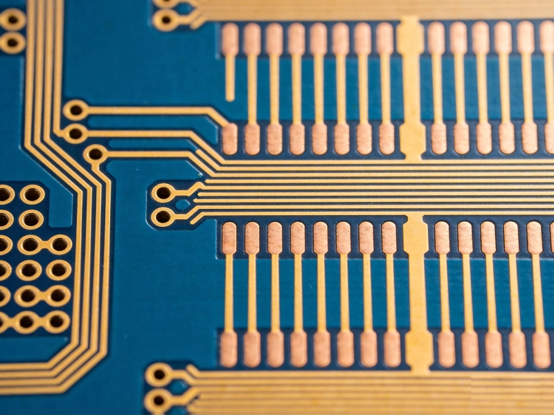
At sub-THz frequencies, trace dimensions affect performance in ways that matter at the micron level. We've developed precision etching processes that maintain trace width tolerances down to ±5 μm on critical signal paths. This level of control enables impedance tolerances of ±3% or better.
Our precision fabrication capabilities:
For 6G research, we often fabricate test structures alongside production traces. These let researchers measure actual fabricated dimensions and correlate with electrical performance. The data helps optimize designs for our fabrication capabilities and builds confidence that final boards will perform as expected.
Conductor surface roughness becomes critical at high frequencies due to Skin Effect. Our standard process uses low-profile copper foil with surface roughness below 1 μm. For the most demanding applications, we offer additional surface smoothing processes that reduce roughness even further.
Surface treatment options:
We've measured insertion loss differences of several dB at 100+ GHz between boards with standard copper and our optimized surface treatments. For research applications where every dB matters, surface treatment selection can be as important as material selection.
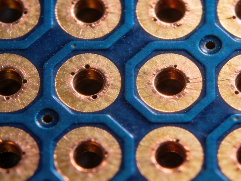
Via stubs cause resonance problems that become severe at sub-THz frequencies. We've developed back-drilling capabilities with depth control accuracy of ±25 μm. This precision ensures stubs are removed completely without damaging adjacent structures.
Our back-drilling capabilities:
For 6G research boards, we often back-drill every via on critical signal paths. The process is time-consuming, but it eliminates stub resonance that would otherwise corrupt measurements at sub-THz frequencies.
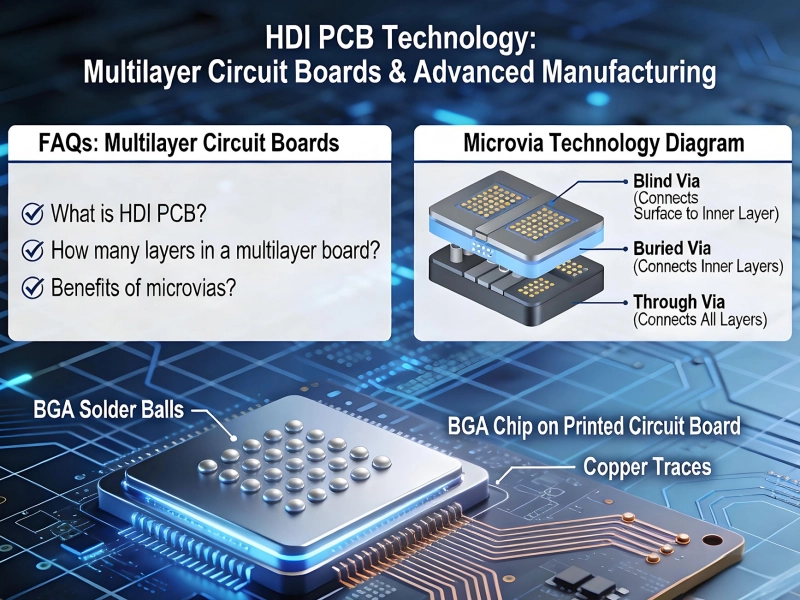
For the highest frequency signal paths, we offer laser-drilled microvias as an alternative to mechanical drilling. Laser vias have smaller diameters and cleaner profiles, reducing parasitic effects that matter at sub-THz frequencies.
Microvia capabilities:
Researchers developing 6G antenna arrays and phased array systems often need dense interconnects between multiple layers. Our microvia capabilities support these designs while maintaining Signal Integrity at extreme frequencies.
Standard high frequency fabrication typically achieves impedance tolerances around ±5-7%. For 6G research, we've developed processes that reliably deliver ±3% tolerance, with ±2% achievable for critical paths on well-designed boards.
Factors enabling tight tolerance control:
Tight impedance tolerance ain't just about fabrication - it requires cooperation between design and manufacturing. We work with research teams during design development to ensure trace geometries, layer stack-ups, and material selections support our fabrication capabilities. This collaborative approach consistently delivers better Impedance Control than boards designed without fabrication input.
At sub-THz frequencies, impedance varies with frequency in ways that don't matter at lower frequencies. Our measurement capabilities include frequency-domain impedance profiling that reveals how transmission lines behave across the full frequency range of interest.
Impedance measurement capabilities:
For research applications, we provide detailed impedance measurement reports that show performance at multiple frequencies. This data helps researchers understand whether boards will perform adequately at target operating frequencies before they invest in expensive measurement campaigns.
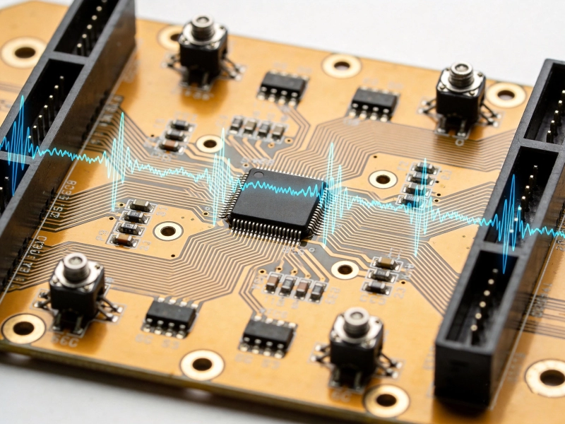
6G research often involves integrated antenna structures on PCBs. We've developed fabrication techniques for various antenna types, from simple patch antennas to complex phased array structures.
Antenna structure capabilities:
Antenna structures require dimensional precision beyond regular PCB traces. Element sizes, spacing, and feed network geometries all affect antenna performance. We fabricate these structures with the same precision control we use for high frequency transmission lines.
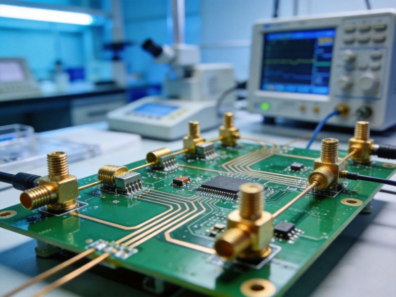
Research boards often need specialized test structures for characterizing materials, processes, or component performance. We fabricate custom test structures alongside production circuits, enabling researchers to extract measurement data from the same boards they use for experiments.
Common test structure types:
We work with researchers to design test structures that extract the data they need while fitting within fabrication constraints. This collaborative approach has helped multiple research teams develop measurement methodologies that actually work on fabricated boards.
Research work needs thorough documentation. We provide detailed fabrication reports that cover materials used, process parameters, dimensional measurements, and electrical test results. This documentation supports research publications and enables traceability for future work.
Documentation we provide:
When researchers are publishing results or building on previous work, they need confidence that boards were fabricated as specified. Our documentation gives them that confidence and provides data for analysis when results don't match expectations.
When research boards don't perform as expected, figuring out why matters. We provide failure analysis support that examines both fabrication quality and design factors. This helps researchers understand whether problems come from fabrication issues, design limitations, or something else entirely.
Failure analysis capabilities:
We've learned a lot from failure analysis work. Problems that seem like fabrication defects sometimes turn out to be design limitations that only manifest at extreme frequencies. This feedback loop between fabrication, testing, and design has driven many of our capability improvements.
We're not just a fabrication vendor - we're a capability partner for 6G research. Our experience with extreme frequency PCBs, ultra-low loss materials, and precision fabrication techniques helps research teams succeed with challenging projects.
How we support research teams:
Research projects often have requirements that evolve as work progresses. We adapt our fabrication approaches as needs change, supporting the iterative nature of experimental work. This flexibility has made us a preferred partner for multiple 6G research programs.
If your 6G research needs PCB capabilities beyond what standard fabrication offers, we're ready to help. Our technical team can discuss your specific requirements and explain how our capabilities address the challenges of sub-THz frequency work.
Contact us to discuss your project: We'll review your design requirements, material needs, and performance targets to develop a fabrication approach that supports your research objectives. From prototype fabrication to production runs for experimental campaigns, we have the capabilities and experience to help you push the limits of 6G technology.
6G research is pushing wireless technology into frequency ranges where standard PCB fabrication can't keep up. We've developed capabilities specifically for these extreme requirements - ultra-low loss materials, precision fabrication, tight impedance control, advanced via structures, and comprehensive quality assurance.
Our work with 6G research teams has taught us what capabilities actually matter. It ain't just about having fancy equipment - it's about understanding the challenges researchers face and developing fabrication approaches that address them. Precision control, reliable processes, thorough documentation, and collaborative support are what make the difference between boards that work and boards that don't.
As 6G research continues pushing toward higher frequencies and more demanding requirements, we're continuing to push our capabilities further. The limits we're pushing today will become standard capabilities tomorrow, enabling even more ambitious research and ultimately commercial 6G systems. We're committed to being part of that evolution, providing the PCB foundation that makes 6G technology possible.
Q: What frequency range can your high frequency PCBs support?
A: Our capabilities support PCBs operating into the sub-THz range (100+ GHz). We've fabricated boards for research applications at frequencies exceeding 200 GHz. Performance depends on material selection, trace geometry, and design optimization for specific frequency requirements.
Q: What impedance tolerances can you achieve for 6G research boards?
A: We reliably achieve ±3% impedance tolerance for well-designed boards. For critical signal paths with optimized geometry and material selection, ±2% tolerance is achievable. Tighter tolerances require design collaboration during development.
Q: Do you support custom material development for specialized research?
A: Yes, we work with research teams that have material requirements beyond standard laminates. We can source specialty materials, develop custom stack-ups, and create fabrication processes for unique material combinations.
Q: What documentation do you provide with research-grade PCBs?
A: We provide comprehensive fabrication reports including material certificates, process records, dimensional measurements, electrical test results, and cross-section documentation when needed. This documentation supports research publications and enables traceability.
Q: Can you fabricate antenna structures integrated with high frequency PCBs?
A: Yes, we have capabilities for integrated antenna structures including patch antennas, feed networks, and phased array support. Antenna structures receive the same precision fabrication treatment as high frequency transmission lines.

Why Advanced Testing Equipment Defines Top High Frequency PCB CapabilitiesJuly/07/2026
Understanding High Frequency PCB Capabilities: Line Width, Spacing, and Layer CountJune/28/2026

High Frequency PCB Capabilities for Aerospace and Defense ApplicationsJuly/17/2026
Pushing the Limits: Our Latest High Frequency PCB Capabilities for 6G ResearchJune/11/2026
Why Component Placement is Critical in High Frequency PCB AssemblyJune/25/2026
The Benefits of Rapid High Frequency PCB PrototypingMay/29/2026
Laser Drilling and Microvias in Modern High Frequency PCB FabricationJuly/07/2026
High Frequency PCB Assembly Best Practices for 5G and RF ModulesJune/08/2026