In the rapidly evolving world of electronics, high frequency applications—from 5g Telecommunications to advanced radar systems—demand precision engineering at every level. While component selection and Pcb Materials receive significant attention, one critical factor often determines the success or failure of high frequency designs: component placement. Strategic component placement isn't just about fitting components onto a board; it's about managing electromagnetic fields, minimizing signal degradation, and ensuring reliable performance at GHz frequencies.
As signal frequencies increase beyond 1 GHz, the physics of signal propagation changes dramatically. What works in low frequency designs can lead to catastrophic failures in high frequency applications. This comprehensive guide explores why component placement is fundamental to High Frequency Pcb Assembly success and provides actionable insights for optimizing your designs.

Understanding High Frequency Signal Behavior
Before diving into placement strategies, it's essential to understand how signals behave at high frequencies. At low frequencies, signals travel instantaneously across traces, and components can be placed relatively freely. However, as frequencies increase into the hundreds of MHz and GHz range, several phenomena become significant:
- Transmission Line Effects: Signal propagation becomes comparable to trace length, requiring Controlled Impedance matching. Signals no longer behave like simple DC circuits but as electromagnetic waves traveling along transmission lines.
- Parasitic Effects: Component leads, traces, and vias introduce parasitic inductance and capacitance that become significant at high frequencies. A 1nH parasitic inductance that's negligible at 100MHz presents significant impedance at 1GHz.
- EMI and Radiation: High frequency signals can radiate electromagnetic energy, causing interference with nearby circuits and violating regulatory requirements. Component placement directly affects radiation patterns and coupling.
- Skin Effect: Current concentrates near conductor surfaces at high frequencies, affecting trace resistance and requiring wider traces or thicker copper to maintain current carrying capacity.
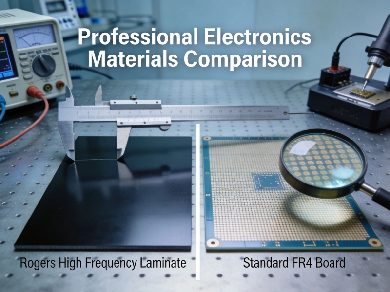
- Dielectric Losses: Pcb Materials become lossy at high frequencies, with signal attenuation increasing with frequency and distance. Proper placement can minimize trace lengths and reduce these losses.
Signal Integrity Fundamentals
Signal Integrity (SI) is the cornerstone of high frequency design, and component placement is the primary lever for maintaining SI. Poor placement leads to signal degradation, timing errors, and complete system failures. The key SI considerations include:
- Impedance Matching: Source and load impedances must match the characteristic impedance of transmission lines to prevent reflections. Component placement affects trace lengths, which impacts Impedance Control and matching networks.
- Crosstalk: Unwanted coupling between adjacent signals can cause interference and errors. Component placement determines trace routing and proximity, directly influencing crosstalk magnitude.
- Signal Degradation: Long trace lengths introduce losses, dispersion, and group delay variations. Strategic placement minimizes critical path lengths, preserving signal quality.
- Timing Closure: For digital systems, trace length matching between differential pairs and clock/data paths is critical. Component placement dictates feasible routing and length matching possibilities.
- Return Path Continuity: High frequency return currents follow the path of least impedance, typically closely coupled to signal traces. Component placement affects ground plane continuity and return path quality.
Component Placement for Power Distribution
Power distribution networks (PDN) in high frequency designs require meticulous component placement to ensure stable voltage delivery and minimize noise. Decoupling capacitors—often called bypass capacitors—are particularly sensitive to placement:
- Decoupling Capacitor Placement: Place decoupling capacitors as close as possible to IC power pins, with the shortest possible loop area between capacitor, power pin, and ground plane. The loop inductance directly determines the capacitor's effectiveness at high frequencies.
- Multiple Decoupling Values: Use multiple capacitor values (e.g., 0.1μF, 0.01μF, 100pF) placed progressively closer to IC pins to address different frequency ranges. Each capacitor's self-resonant frequency determines its effective frequency range.
- Power Entry Points: Position power connectors and bulk capacitors near board edges where power enters the design, establishing a stable reference point for the PDN.
- Voltage Regulator Placement: Locate voltage regulators near the components they serve, minimizing distribution losses and improving transient response. Consider thermal requirements in placement decisions.
- Ground Plane Management: Maintain continuous ground planes beneath power components and traces to provide low-impedance return paths and reduce noise coupling.
Minimizing Electromagnetic Interference (EMI)
EMI control is perhaps the most challenging aspect of high frequency design, and component placement is the first line of defense against radiation and susceptibility issues:
- Differential Pair Spacing: Place differential signal components to enable tight coupling between positive and negative traces, canceling electromagnetic fields and reducing radiation. Maintain consistent spacing throughout the routing.
- High Frequency Source Isolation: Position high frequency signal sources (oscillators, clock generators) away from sensitive analog circuits, connectors, and board edges where radiation might escape.
- Shielding Components: Place EMI-sensitive components (filters, ferrite beads, shielding cans) at board entry points or between noise sources and sensitive circuits to block interference.
- Ground Plane Discontinuities: Avoid placing components over ground plane splits or slots that disrupt return current paths. Route high frequency traces over continuous ground reference planes.
- Connector Placement: Position connectors (especially for external cables) at board edges and use EMI filters nearby to prevent noise from radiating through cables. Provide adequate ground connections for connector shells.
Thermal Considerations in Component Placement
High frequency components often generate significant heat, and thermal management directly impacts electrical performance and reliability. Component placement must balance electrical and thermal requirements:
- Power Dissipation Distribution: Spread heat-generating components across the board to prevent hot spots that can degrade performance and reduce component lifespan. Consider board thermal conductivity and airflow patterns.
- Thermal Coupling: Isolate temperature-sensitive components (precision analog ICs, oscillators) from heat sources, or provide thermal isolation through spacing, thermal relief patterns, or physical barriers.
- Ventilation and Airflow: Position components considering the enclosure's airflow patterns. Place tall or high-power components where airflow is unobstructed, avoiding shadowing effects.
- Thermal Vias: Plan thermal via placement under heat-generating components to conduct heat to inner ground planes or opposite board layers. Thermal vias should be placed in arrays for optimal heat transfer.
- Component Height: Consider component height and placement relative to enclosure features, lids, or other components that might impede airflow or thermal radiation.
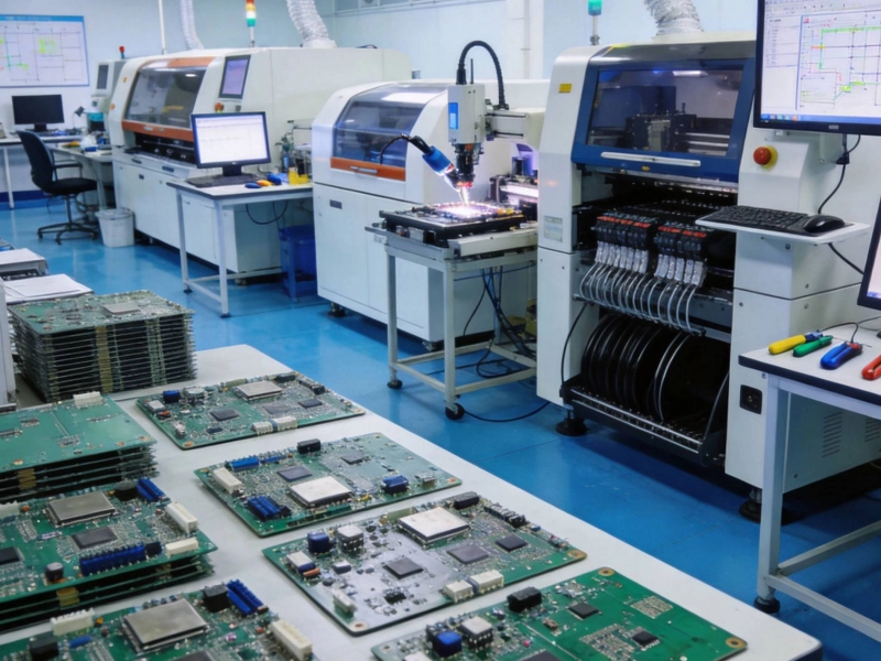
Manufacturing and Assembly Optimization
While electrical performance is paramount, component placement must also consider manufacturability and assembly yield. Well-placed components improve assembly efficiency and reduce defect rates:
- Component Orientation: Orient polarized components (diodes, capacitors, ICs) consistently to reduce assembly errors and improve inspection efficiency. Standard orientation also helps reduce placement time.
- Spacing and Clearance: Maintain adequate spacing between components to accommodate solder paste application, inspection, rework, and conformal coating if required. Consider equipment constraints and inspection requirements.
- Component Grouping: Group related components together (e.g., all resistors in a filter network, all decoupling capacitors for an IC) to simplify routing, reduce trace lengths, and improve manufacturability.
- Test Point Access: Place test points in accessible locations for ICT, flying probe, or boundary scan testing. Ensure test points aren't shadowed by tall components.
- Rework Considerations: Consider component reworkability in placement. Provide access for hot air rework tools and avoid placing heat-sensitive components near difficult-to-replace components.
High Frequency Component Placement Best Practices
Based on successful high frequency designs across various applications, several placement best practices have emerged:
- Signal Flow Architecture: Arrange components following the natural signal flow from input to output, minimizing backtrack routing and keeping signal paths as direct as possible.
- Critical Path Optimization: Identify the most critical high frequency paths (clock signals, high-speed data interfaces) and prioritize component placement to minimize these trace lengths first.
- Ground Reference Consistency: Keep high frequency components over continuous ground reference planes. Avoid ground plane discontinuities under high frequency components and traces.
- Via Minimization: Minimize vias in high frequency signal paths as they introduce parasitic inductance and capacitance. When vias are necessary, use appropriate via structures (back-drilling, blind vias) to minimize their impact.
- Edge Distance: Keep high frequency components and traces away from board edges where EMI can radiate more easily and where mechanical stress might affect performance.
- Layer Utilization: Use inner layers for high frequency routing where possible, taking advantage of better Impedance Control and reduced EMI radiation compared to outer layers.
- Component Size Matching: Match component package sizes to routing density requirements. Use smaller packages (0402, 0201) where density is needed, larger packages where assembly yield is priority.
Digital High Frequency Considerations
Digital systems operating at high frequencies present unique placement challenges, particularly regarding timing and Signal Integrity:
- Clock Distribution: Place clock generators and buffers centrally, with fan-out traces radiating equally to destination components. Ensure clock paths are the shortest traces on the board.
- DDR Memory Placement: Position DDR memory components as close as possible to memory controllers, with matched trace lengths for address, data, and control signals. Consider both length matching and phase matching.
- High-Speed Serial Links: For SerDes interfaces (PCIe, USB, SATA), place serializers/deserializers close to connectors, with careful impedance control and length matching within tolerance specifications.
- Termination Placement: Place termination resistors at the exact location specified in interface standards (typically near receivers for source termination, near drivers for parallel termination).
- Ground Reference Switching: Avoid routing high frequency signals across ground plane splits or between different ground reference areas. If unavoidable, provide proper bridging and consider reference plane stitching capacitors.
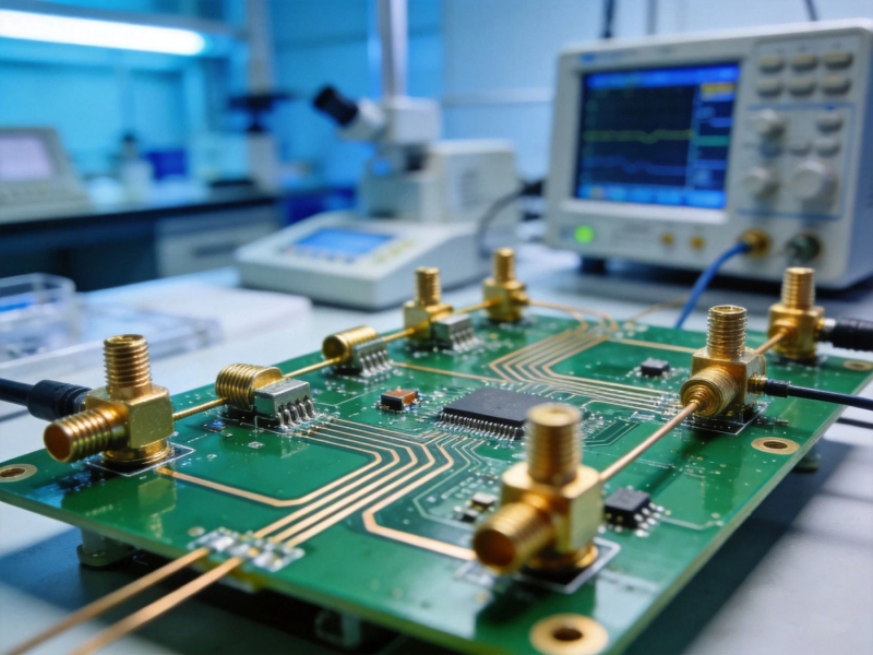
RF and Microwave Placement Strategies
RF and microwave circuits (typically above 500MHz) demand the most stringent placement practices due to extreme sensitivity to parasitic effects:
- Filter Placement: Place RF filters immediately at the input/output of RF chains, with minimal trace length before and after the filter. Any trace length adds insertion loss and affects filter performance.
- Impedance Matching Networks: Place matching networks as close as possible to the device pins they're matching. Any additional trace length becomes part of the matching network and can disrupt intended performance.
- Shielded Compartment Design: Design placement to allow for shielding cans or metal compartments around sensitive Rf Circuits. Consider compartment size, feedthrough placement, and ground connections.
- Transistor Placement: Place RF transistors (especially in amplifier and mixer stages) considering thermal requirements, input/output spacing, and ground return paths. Heat sinking requirements often conflict with optimal RF placement.
- Connector-to-Circuit Distance: Minimize distance between RF connectors and the first active component in the chain. Any interconnect length becomes part of the RF circuit and must be characterized in the design.
Analog High Frequency Considerations
Analog circuits operating at high frequencies require placement strategies that preserve signal fidelity and minimize noise:
- Operational Amplifier Placement: Place op-amps as close as possible to their feedback networks to minimize parasitic inductance and capacitance that can cause oscillation or frequency response degradation.
- Reference Voltage Sources: Position precision voltage reference sources away from noise sources and switching circuits, with dedicated filtering and ground connections.
- Input/Output Separation: Maintain clear separation between sensitive analog input circuits and potentially noisy output circuits to prevent feedback and oscillation.
- Guard Rings: Implement guard rings around high impedance input nodes, connected to the appropriate potential, to prevent leakage currents and interference.
- Ground Partitioning: For mixed analog/digital designs, carefully partition ground areas and manage placement to avoid digital currents flowing through sensitive analog ground regions.
Validation and Verification of Placement
Once component placement is complete, thorough validation is essential before proceeding to routing and fabrication:
- 3D Visualization: Use 3D visualization tools to check for component collisions, mechanical interferences, and proper spacing within the enclosure.
- Electrical Simulation: Perform electromagnetic field simulations (S-parameter analysis, EMI/EMC analysis) on critical placements to validate signal integrity and radiation performance.
- Thermal Simulation: Run thermal analysis to ensure component temperatures remain within specifications and that thermal gradients don't affect sensitive circuits.
- Design Rule Checking: Run comprehensive DRC checks covering spacing, clearance, manufacturing constraints, and high frequency-specific rules.
- Prototype Review: Review placement with assembly and test engineers to identify potential issues before fabrication. Their practical experience often catches problems simulation might miss.
Common Placement Mistakes to Avoid
Learning from others' mistakes can prevent costly redesigns and iterations:
- Decoupling Capacitor Distance: One of the most common mistakes is placing decoupling capacitors too far from IC power pins, rendering them ineffective at high frequencies.
- Ground Plane Disruption: Placing components or traces over ground plane splits or slots creates unpredictable impedance and return path issues.
- Trace Length Neglect: Failing to minimize critical high frequency trace lengths leads to excessive loss, phase shifts, and potential timing violations.
- Differential Pair Separation: Increasing spacing between differential pair traces to route around obstacles reduces field cancellation and increases radiation.
- Component Height Overlook: Not considering component height in placement leads to mechanical interferences with enclosure features, heatsinks, or other components.
- Test Point Inaccessibility: Placing test points in inaccessible locations makes post-assembly testing difficult or impossible, reducing test coverage.
Future Trends and Emerging Technologies
As frequencies continue to increase and applications become more demanding, component placement strategies are evolving:
- mmWave and Terahertz Frequencies: At frequencies above 30GHz, component placement becomes even more critical with wavelengths measured in millimeters. Placement tolerances tighten dramatically.
- Advanced Packaging: System-in-Package (SiP) and 3D IC integration reduce interconnect lengths but introduce new placement challenges for package-level interconnects.
- AI-Assisted Placement: Machine learning algorithms are being developed to optimize component placement for multiple objectives (signal integrity, thermal, manufacturability) simultaneously.
- Embedded Components: Technology is moving toward embedding passive components within PCB layers, requiring new placement paradigms that consider internal component locations.
- Integrated Passive Devices: Integration of multiple passive components into single packages simplifies placement but requires understanding the internal layout for optimal external placement.
Conclusion
Component placement in High Frequency Pcb Assembly is not merely a layout exercise—it's a critical design discipline that determines electrical performance, reliability, and manufacturability. The physics of high frequency signals transforms what seems like minor placement decisions into significant performance factors. Every millimeter of trace length, every parasitic inductance, and every return path discontinuity compounds to affect signal integrity and EMI performance.
Successful high frequency designs require balancing multiple competing requirements: signal integrity, EMI control, thermal management, and manufacturability. Strategic component placement addresses these requirements at the foundation level, creating a solid platform for successful routing and implementation. As frequencies continue to increase and applications become more demanding, the importance of meticulous component placement only grows.
By understanding the principles outlined in this guide and implementing best practices for your specific application, you can achieve optimal performance from your High Frequency Pcb assemblies while minimizing design iterations and manufacturing issues. Remember that in high frequency design, placement is not just about fitting components—it's about engineering the electromagnetic environment for optimal performance.
FAQ
Q: How close should decoupling capacitors be placed to IC power pins?
A: For high frequency applications, decoupling capacitors should be placed within 1-2mm of IC power pins, with the shortest possible loop area. The via from capacitor ground pad to ground plane should also be as close as possible to minimize inductance. For frequencies above 100MHz, 0.1μF capacitors should be within 2mm, 0.01μF within 1mm, and 100pF capacitors should be placed immediately adjacent to power pins.
Q: Can I use automatic component placement tools for high frequency designs?
A: While automatic placement tools can provide starting points, high frequency designs typically require manual placement for critical components. Automated tools rarely understand signal integrity, EMI, and thermal requirements adequately. Use auto-placement for non-critical components, then manually place high frequency components (clocks, serializers, RF front-ends) following the principles outlined in this guide.
Q: What's the maximum trace length for a 1GHz signal?
A: There's no single maximum length—it depends on your specific application requirements and acceptable signal degradation. However, as a general rule, at 1GHz, traces should be kept as short as possible, ideally under 25mm for critical signals. For differential pairs, length matching tolerances typically require matching within 5-10 mils. Use signal integrity simulation tools to determine acceptable lengths based on your specific requirements.
Q: How do I handle component placement when I have space constraints?
A: When space is limited, prioritize placement based on criticality. Place the most sensitive high frequency components first (clocks, RF front-ends, high-speed serializers), then fit other components around them. Consider using smaller component packages (0402, 0201) for high density areas. Be prepared to iterate placement multiple times to find an optimal arrangement that balances all requirements.
Q: Should I place components before or after defining layer stack-up?
A: Layer stack-up should be defined before component placement because it influences placement decisions. The number of signal layers, ground planes, and power planes affects routing density, reference plane availability, and EMI considerations. Having the stack-up defined allows you to place components with understanding of which layers will be available for routing and where ground reference planes exist.
Q: How does component placement affect PCB cost?
A: Component placement influences PCB cost through several mechanisms: smaller component packages (better for high frequency designs) are often more expensive, complex placement requiring more layers increases board cost, and placement that requires special manufacturing processes (blind vias, back-drilling) adds cost. However, good placement that reduces defects and improves yield can offset these costs. Balance placement optimization against overall project cost constraints.
Q: What tools should I use for verifying component placement in high frequency designs?
A: A combination of tools is recommended: use your PCB design software's 3D viewer for mechanical verification, electromagnetic simulation tools (ADS, CST, HFSS) for signal integrity and EMI analysis, thermal analysis tools for temperature distribution, and design rule checking for manufacturing constraints. Each tool validates different aspects of placement quality.
Are you designing a High Frequency Pcb and want to ensure optimal component placement for maximum performance and reliability? Partner with experienced PCB design and assembly specialists who understand the complexities of high frequency applications and can help you achieve design success on the first iteration.