

In the rapidly evolving world of electronics, high frequency applications—from 5G telecommunications to advanced radar systems—demand precision engineering at every level. While component selection and PCB materials receive significant attention, o...
https://www.high-frequency-pcb.com/high-frequency-pcb-assembly/why-component-placement-is-critical-in-high-frequency-pcb-assembly/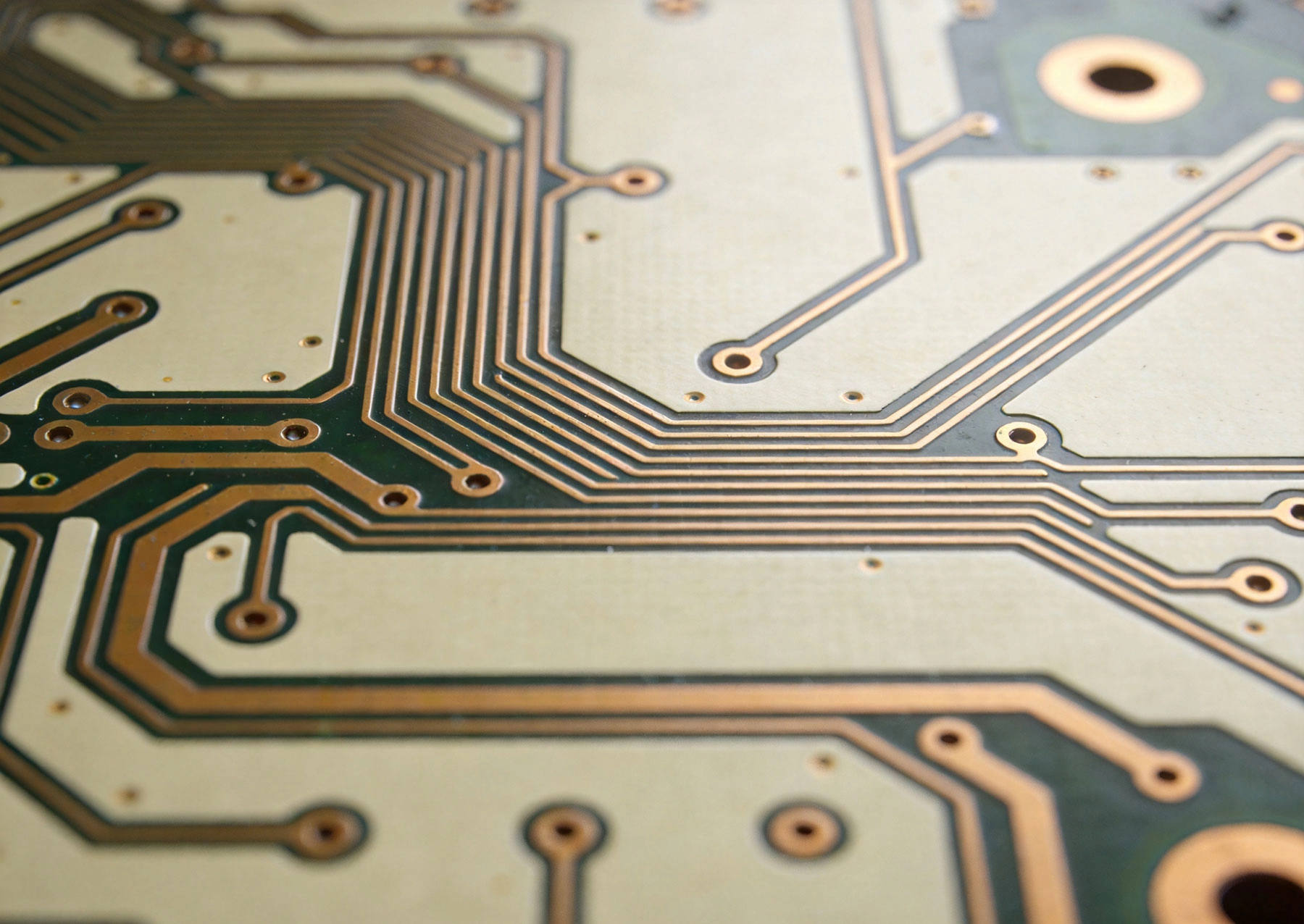
Ask any engineer who has designed a high-speed digital board or an RF frontend, and they will tell you the same thing: getting impedance control right is one of those topics that looks deceptively simple on the surface and reveals hidden complexity...
https://www.high-frequency-pcb.com/high-frequency-pcb-knowledge/demystifying-impedance-control-core-high-frequency-pcb-knowledge/
Aerospace and defense systems operate at the cutting edge of high-frequency technology. Radar systems operating at X-band and Ka-band frequencies, satellite communications spanning multiple gigahertz, electronic warfare systems jamming across wide ...
https://www.high-frequency-pcb.com/high-frequency-pcb-capabilities/high-frequency-pcb-capabilities-for-aerospace-and-defense-applications/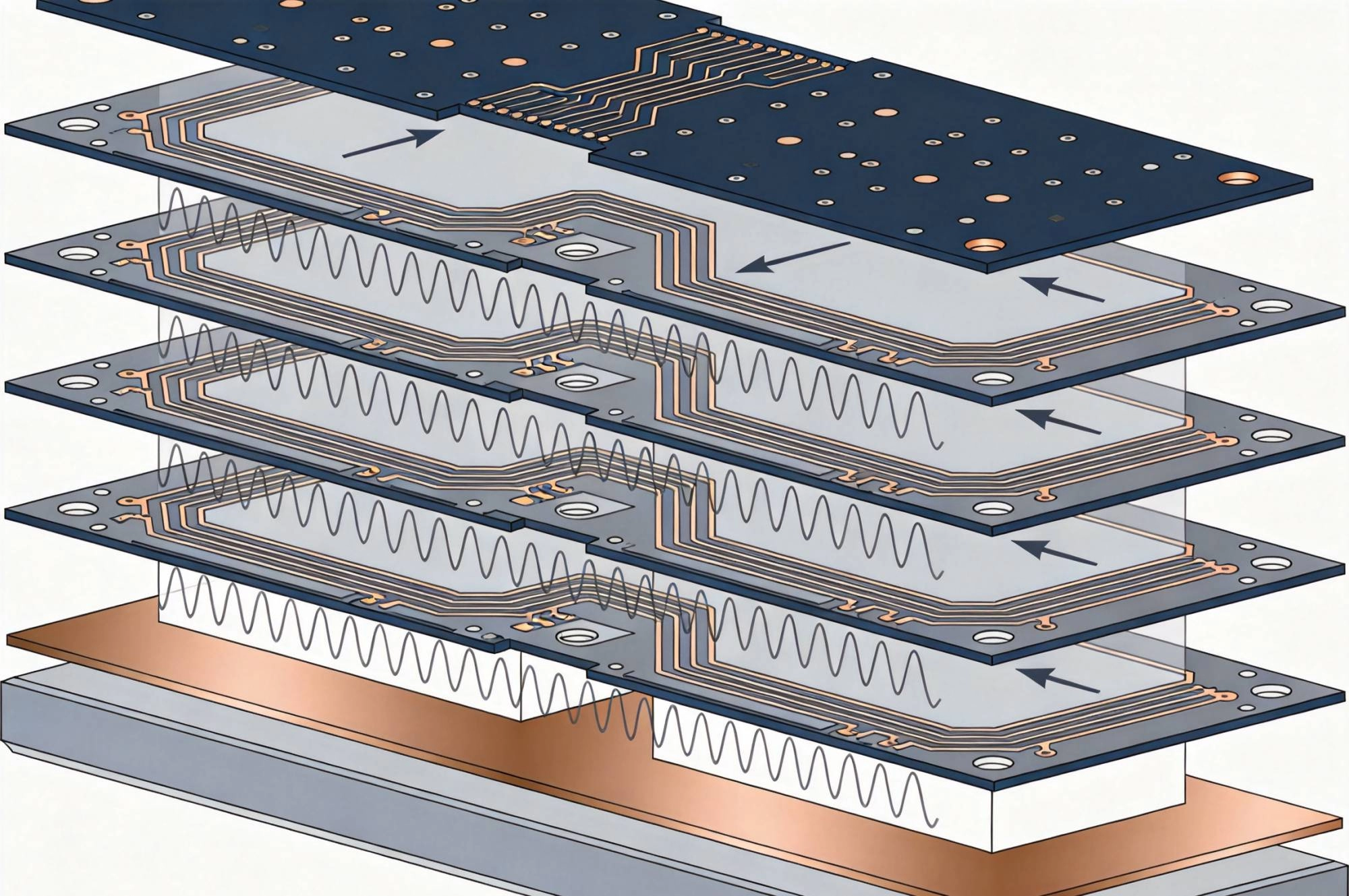
High frequency printed circuit boards operate under rules that differ fundamentally from those governing low-speed digital designs. At frequencies above approximately 1 GHz, trace dimensions become comparable to signal wavelengths, transforming PCB...
https://www.high-frequency-pcb.com/high-frequency-pcb-knowledge/the-engineers-guide-to-high-frequency-pcb-knowledge-and-stack-up-design/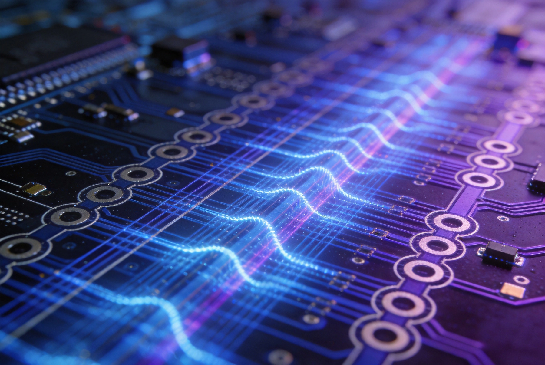
Every signal on a PCB is accompanied by an electromagnetic field. At low frequencies and slow edge rates, those fields are a rounding error — they exist, technically, but they do not cause problems that show up on oscilloscopes or bit error rate te...
https://www.high-frequency-pcb.com/high-frequency-pcb-knowledge/high-frequency-pcb-knowledge-managing-crosstalk-and-emi-in-dense-layouts/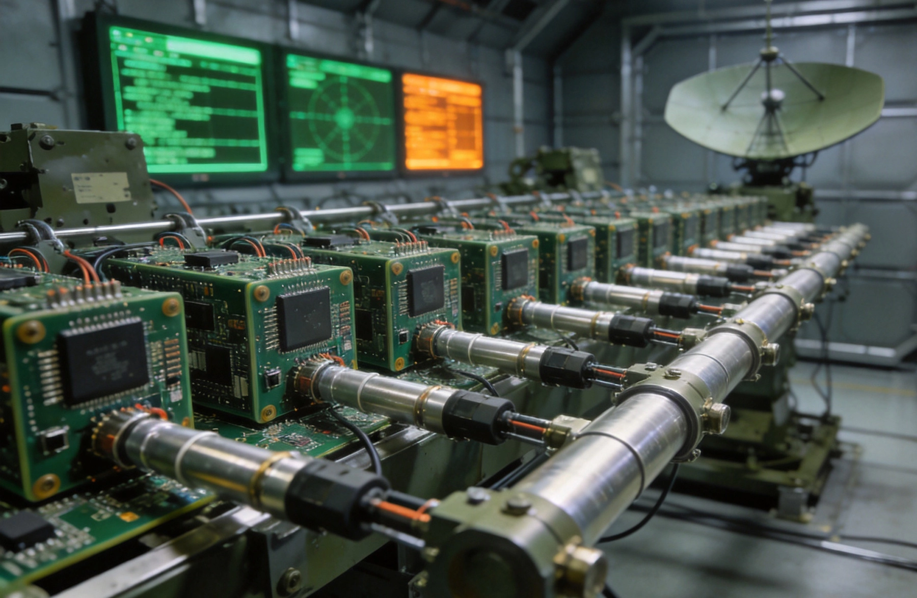
Modern military radar and electronic warfare systems operate at frequencies that would have been considered science fiction a generation ago. Phased array radars operating in X-band (8–12 GHz), Ka-band (26–40 GHz), and even W-band (75–110 GHz) are ...
https://www.high-frequency-pcb.com/energy-power-electronics/high-frequency-pcb-applications-for-military-radar-and-electronic-warfare/