Open Nav

Modern military radar and electronic warfare systems operate at frequencies that would have been considered science fiction a generation ago. Phased array radars operating in X-band (8–12 GHz), Ka-band (26–40 GHz), and even W-band (75–110 GHz) are now standard in ground-based air Defense Systems, naval fire control radars, and airborne surveillance platforms. Electronic warfare systems — jammers, decoys, and electronic support measures — operate across the same spectrum and beyond, often pushing into sub-Millimeter Wave frequencies as the electromagnetic battlespace becomes more contested.
At these frequencies, the printed circuit board is not merely a substrate for mounting components. It is an integral part of the RF signal path — carrying high-frequency energy between amplifiers, filters, beamforming networks, and antennas with minimal loss, predictable impedance, and immunity to interference. Designing and manufacturing PCBs for these applications demands a level of engineering precision, material performance, and process control that is fundamentally different from standard digital or Power Electronics. This article explores what that means in practice.
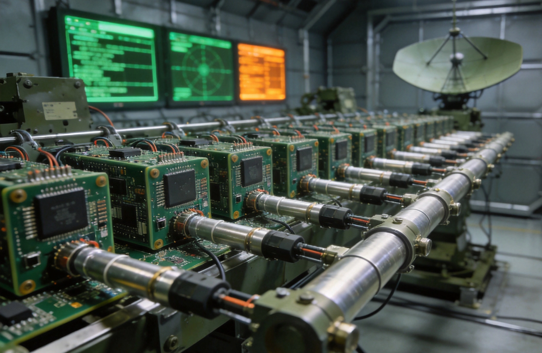
At low frequencies — below 1 GHz — the electrical behavior of a PCB is forgiving. Traces behave like simple conductors, vias are negligible inductors, and most material properties are close to constants. As frequency rises into the microwave and millimeter-wave bands, every physical feature of the PCB becomes an electrical element. A trace is a Transmission Line with distributed inductance and capacitance. A via is an impedance discontinuity. The Dielectric Constant of the laminate is no longer a single number — it varies with frequency, temperature, and moisture content.
For military radar and EW applications, this has direct consequences:
Managing these effects requires Pcb Materials, design practices, and manufacturing processes optimized for microwave performance — not just digital performance with better specs.
The PCB substrate material is the single most important determinant of high-frequency electrical performance. Every electrical property of the board — Dielectric Constant, loss tangent, dimensional stability, thermal coefficient of dielectric constant — flows from the choice of laminate.
Two parameters dominate material selection for RF applications:
Dielectric Constant (Dk, εr): The ratio of the material's permittivity to free space. This determines the propagation velocity of signals in the dielectric and sets the impedance of Transmission Lines. Lower Dk materials allow faster signal propagation and wider trace geometry for a given impedance. The Dk must be tightly controlled — variations of even 2–3% across a board cause impedance scatter that degrades performance.
Loss Tangent (Df, tan δ): The ratio of loss to stored energy in the dielectric. Lower loss tangent means less signal attenuation per unit length. At Ka-band and above, this matters enormously: a laminate with Df of 0.003 might be acceptable at X-band but produce unacceptable loss at 77 GHz. Loss tangent also increases with temperature and moisture absorption, so the thermal and hygroscopic stability of the laminate is as important as the baseline value.
Standard Fr-4 has Dk of approximately 4.4 and Df of 0.02 — acceptable for digital signals up to a few hundred megahertz, but unsuitable for RF applications above a few GHz. Military radar and EW systems use one of the following high-performance RF laminates:
Military radar and EW boards are rarely purely RF. They include digital processing sections running at multi-Gbps data rates, power distribution networks, beamforming control circuits, and thermal management structures. A practical approach combines materials strategically: Rogers or Taconic for RF sections, Megtron 6 or equivalent for high-speed digital sections, and standard or high-Tg Fr-4 for power layers where RF performance is irrelevant.
This hybrid approach requires careful interface design where the different materials meet. The thermal expansion mismatch between PTFE and FR-4 can create stress during temperature cycling, so the interface — typically a step-lapped or bonded construction — must be designed to manage this. The bonding process for hybrid constructions also requires compatibility with both material types, which can be challenging for some prepreg and bonding film options.
Controlling impedance in high-frequency PCBs is not a nice-to-have — it is an absolute requirement. At Ka-band, a 1-ohm impedance mismatch on a 50-ohm Transmission Line causes a reflection coefficient of about 2% — small in percentage terms but enough to create measurable power loss and VSWR degradation in a sensitive radar receiver.
Microstrip and grounded coplanar waveguide (GCPW) are the most common transmission line geometries for military RF PCBs. Each has advantages:
Microstrip: A signal trace on an outer layer with a ground plane below. Simple to manufacture and analyze. Susceptible to crosstalk from adjacent traces and radiation from the top surface. Impedance is determined by trace width, dielectric thickness, and copper weight — with Dk held constant, these parameters must be controlled to tight tolerances.
Grounded Coplanar Waveguide (GCPW): A signal trace flanked by ground strips on the same layer, with a ground plane below. Provides better isolation between adjacent channels, reduces crosstalk, and offers better mode suppression than microstrip. The additional processing step — slots must be etched on either side of the trace — is well within the capability of experienced Rf Pcb fabricators.
The stackup design establishes the dielectric thickness, copper weight, and material Dk that determine impedance. For each target impedance, the geometry — trace width for microstrip, trace width and gap for GCPW — is calculated using electromagnetic simulation tools. Standard 1D calculators (like the IPC-2141A formulas) are adequate for rough design, but final verification requires 2D or full-wave 3D electromagnetic simulation to account for via transitions, connector footprints, and material anisotropy.
At 30 GHz and above, manufacturing tolerances become a critical design parameter. A trace width variation of ±0.05mm — well within normal PCB Fabrication tolerances — causes approximately 0.5–1% impedance variation in a typical microstrip design. This may be acceptable at 10 GHz but problematic at 77 GHz. For W-band applications, tolerances of ±0.02mm or tighter may be required for critical Transmission Lines, necessitating laser trimming, impedance calibration, or statistical process control with 100% impedance testing of finished boards.
Material Dk variation is equally important and harder to control. Rogers Laminates are available with Dk tolerance of ±0.05 for standard grades and tighter for premium grades. Specify the tighter tolerance if Impedance Control is critical. During fabrication, the fab should measure and control etch factor, copper thickness, and prepreg flow to minimize Dk and geometry variation.
Vias are the most disruptive feature in an RF signal path. A through-hole via traversing the board from top to bottom creates an impedance discontinuity — a combination of inductive stub length, parasitic capacitance at the pad, and discontinuity in the ground return path — that degrades return loss and increases Insertion Loss, particularly at millimeter-wave frequencies.
Mitigation strategies include:
Military radar and EW systems routinely include high-power RF amplifiers — GaN (gallium nitride) and GaAs (gallium arsenide) power transistors — that dissipate tens to hundreds of watts in a concentrated area. The thermal environment can be severe: airborne platforms operate at altitude with reduced convective cooling; ground-based systems may operate in desert environments with ambient temperatures exceeding 55°C; naval systems must handle salt spray and high humidity.
Managing heat in military RF PCBs requires specialized thermal management structures:
Insulated Metal Substrate (IMS) boards — with a dielectric layer of 75–150μm between the copper circuit and an aluminum or copper base plate — provide thermal conductivities of 1–5 W/mK in the dielectric layer, enabling heat removal at rates impossible with standard FR-4. IMS is commonly used for power amplifier stages in radar transmitters, where the thermal path from the transistor die through the package, solder joint, IMS dielectric, and base plate to the heatsink determines the maximum operating junction temperature and thus the power handling capability of the stage.
The trade-off with IMS is electrical: the dielectric layer is thin and has dielectric properties that must be characterized for RF applications. Rogers offers metal-base materials (RO4003C LoPro, for example) that provide improved thermal conductivity while maintaining the RF performance of standard Rogers materials.
For multilayer RF boards where IMS is not practical, thermal via arrays provide heat removal through the board stackup. High thermal conductivity paths — thick copper plating in via barrels, copper coin or insert coin technologies — create thermal pathways from the heat source to the board edge or to a heatsink attachment surface. Thermal simulation using tools like Ansys Icepak or Siemens NX Thermal is standard for designing thermal via structures that achieve the required junction temperatures under worst-case power dissipation.
Military radar and EW boards frequently require multilayer constructions to integrate RF signal layers, digital signal layers, power distribution, and DC bias networks into a single assembly. The multilayer stackup must balance RF performance, thermal management, and structural requirements while fitting within tight dimensional envelopes — airborne and shipboard electronics are severely space-constrained.
A typical 8-layer military Radar Pcb stackup might look like:
The key discipline in multilayer RF stackup is isolation: keeping the digital noise from the DC-DC converters and high-speed logic from coupling into the sensitive RF paths. This requires dedicated RF ground planes, careful filtering of any control or bias signals that cross the RF section, and physical separation of noisy circuits from sensitive circuits on the board layout.
PCBs for military radar and EW applications must meet a demanding set of standards that define material performance, design requirements, Manufacturing Quality, and testing procedures. Understanding these standards — and their implications for design and manufacturing — is essential for anyone working in this space.
Military programs typically require documented design verification for RF performance, including:
Manufacturing RF PCBs for military applications requires capabilities and process controls that are well beyond standard PCB Fabrication. Not all RF fabs can reliably produce boards for Ka-band and above, and not all can meet the documentation and Quality Assurance requirements of military programs.
Key manufacturing capabilities to verify when selecting a supplier for military RF PCBs:
Several Chinese PCB manufacturers have developed strong capabilities in high-frequency Rf Pcb fabrication, driven by the growth of 5G infrastructure and domestic defense electronics programs. For commercial radar and EW applications where ITAR (International Traffic in Arms Regulations) restrictions do not apply, qualified Chinese manufacturers can offer cost and lead time advantages over Western sources.
For military programs with ITAR requirements, the manufacturing and supply chain must be ITAR-compliant, which typically restricts manufacturing to ITAR-registered facilities and requires controlled access to technical data. Navigating this requirement carefully — with legal counsel and program office guidance — is essential before engaging non-US manufacturers.
As military radar and EW systems push to higher frequencies and smaller form factors, traditional discrete PCB approaches are being supplemented by System-in-Package (SiP) and Antenna-in-Package (AiP) technologies. These approaches integrate multiple dies, passive components, and in some cases antennas into a single package module — combining functions that would previously have required a full PCB in a footprint a fraction of the size.
SiP and AiP technologies are particularly relevant for:
The PCB implications are significant: these packages require high-density interconnect (HDI) substrates — often build-up multilayer constructions with microvias and fine lines — in addition to the RF expertise already described. The manufacturing and qualification requirements are correspondingly more demanding, and the supply chain is more specialized than for standard PCBs.
High-frequency PCBs for military radar and electronic warfare represent the most demanding end of the PCB performance spectrum. Every parameter — material dielectric constant, trace geometry, via design, plating quality, thermal management — directly affects the electrical performance of the system. There is no room for approximation, no tolerance for shortcuts, and no substitute for engineering rigor at every stage from material selection to final test.
The factories and engineering teams that succeed in this space share a common approach: they treat the PCB as a critical RF component, not as a passive substrate. They invest in EM simulation, thermal analysis, and process control. They select materials based on measured electrical performance data, not just datasheet values. And they build long-term relationships with PCB manufacturers who invest in the capability and quality systems required to deliver performance that can be relied upon in the most demanding operational environments on earth.
For Ka-band (26–40 GHz) radar applications, Rogers Ro4350b is the most widely used commercial material — it offers Dk of 3.48 with tight tolerance (±0.05), Df of 0.0037, and is well-established among experienced RF PCB fabricators. For the lowest loss at these frequencies, Rogers RT/duroid 5880 (Dk 2.2, Df 0.0009) provides superior performance at higher material and manufacturing cost. The choice depends on the link budget — how much insertion loss the system can afford — and the manufacturing and cost constraints of the program.
MIL-PRF-31032 is a performance specification that defines design, materials, and test requirements for rigid PCBs used in military applications. It imposes stricter controls on base material qualification, plating thickness and uniformity, dielectric integrity, and consistency testing than commercial specifications like IPC-6012. It also requires more extensive documentation, traceability records, and incoming/ongoing inspection programs. For space and military radar applications, IPC-6012DS (the Space and Defense addendum) is often specified in addition to or in lieu of MIL-PRF-31032, with specific modifications for high-frequency RF performance requirements.
Back-drilling is a controlled machining process that removes the non-functional portion of a plated through-hole barrel beyond the layer where the signal terminates. A signal via that goes from Layer 1 to Layer 3, for example, would normally have a barrel extending all the way through the board to Layer 8. The unused portion (the "stub") acts as a quarter-wave resonant structure at high frequencies, causing Signal Reflection and loss. Back-drilling removes this stub, leaving only the barrel section that actually carries the signal. For RF applications above 10 GHz, back-drilling or equivalent stub-elimination techniques are essential for maintaining acceptable return loss.
Impedance Control at high frequency requires co-design of the laminate material (Dk, thickness, loss tangent), trace geometry (width, spacing, copper weight), and manufacturing process (etch factor, plating uniformity). Design uses 2D and 3D electromagnetic simulation to calculate geometry for the target impedance. Manufacturing requires tight control of dielectric thickness, trace width, and copper weight — specifying tight tolerances on material Dk, using statistical process control for etch and plating, and verifying impedance on production boards using TDR (Time Domain Reflectometry) testing. For the most demanding applications, individual trace Impedance Measurement on finished boards may be required as 100% inspection rather than statistical sampling.
High-power RF amplifiers in military radar systems — typically GaN or GaAs transistors — require active thermal management to maintain junction temperatures within safe operating limits. Techniques include Insulated Metal Substrate (IMS) constructions with thermal dielectric layers, thermal via arrays with heavy copper plating to conduct heat through the board stackup, copper coin or insert coin technologies that embed high-thermal-conductivity copper structures under the device footprint, and direct liquid cooling attachment points for the highest-power applications. Thermal simulation is essential to predict junction temperatures under worst-case operating conditions, and thermal test coupons are used to verify thermal paths during qualification.
Several Chinese manufacturers have developed strong Rf Pcb Fabrication capabilities for frequencies up to 77 GHz and beyond, driven by 5G infrastructure and domestic defense programs. For programs not subject to ITAR restrictions, qualified Chinese manufacturers can be cost-competitive and technically capable. For ITAR-controlled programs, manufacturing must be conducted in registered ITAR-compliant facilities, which limits options. Regardless of geography, verify the manufacturer's specific experience with the Rf Laminate Materials, frequency range, and tolerance requirements of your application before qualifying them as a supplier.

High Frequency PCB Knowledge: How to Minimize Insertion Loss and ReflectionJuly/21/2026
The Ultimate Guide to High Frequency PCB Materials: PTFE, Ceramic, and HydrocarbonJuly/08/2026
The Rise of High Frequency PCB Applications in IoT and Smart Home DevicesSeptember/08/2026
The Importance of Thermal Management in High Frequency PCB AssemblyJuly/27/2026
Choosing the Right High Frequency PCB MaterialsMay/29/2026

Essential High Frequency PCB Knowledge for Hardware Engineers and DesignersJune/15/2026
High Frequency PCB Fabrication: Managing Dielectric Constant (Dk) TolerancesJune/09/2026
Common Pitfalls to Avoid During Your High Frequency PCB Prototype PhaseJune/18/2026