Open Nav

high frequency PCB assembly operates at the intersection of electrical performance and thermal physics. While Signal Integrity, Impedance Control, and dielectric losses dominate the conversation in high-frequency design, Thermal Management remains the silent foundation that determines whether carefully engineered electrical performance translates into reliable field operation. Heat generated by power dissipation, signal losses, and component operation accumulates in the PCB structure, and without deliberate Thermal Management strategies, this heat degrades electrical performance, accelerates material aging, and ultimately causes premature failures. Understanding thermal management is essential for anyone designing, assembling, or maintaining high-frequency electronic systems.
This article examines why thermal management matters specifically in high-frequency applications, explores the unique thermal challenges these applications present, and provides practical strategies for effective heat dissipation in High-frequency Pcb assemblies. Whether you're designing 5G front-end modules, Millimeter Wave antennas, or high-speed digital systems, the thermal management principles described here will help you create more reliable, better-performing products.
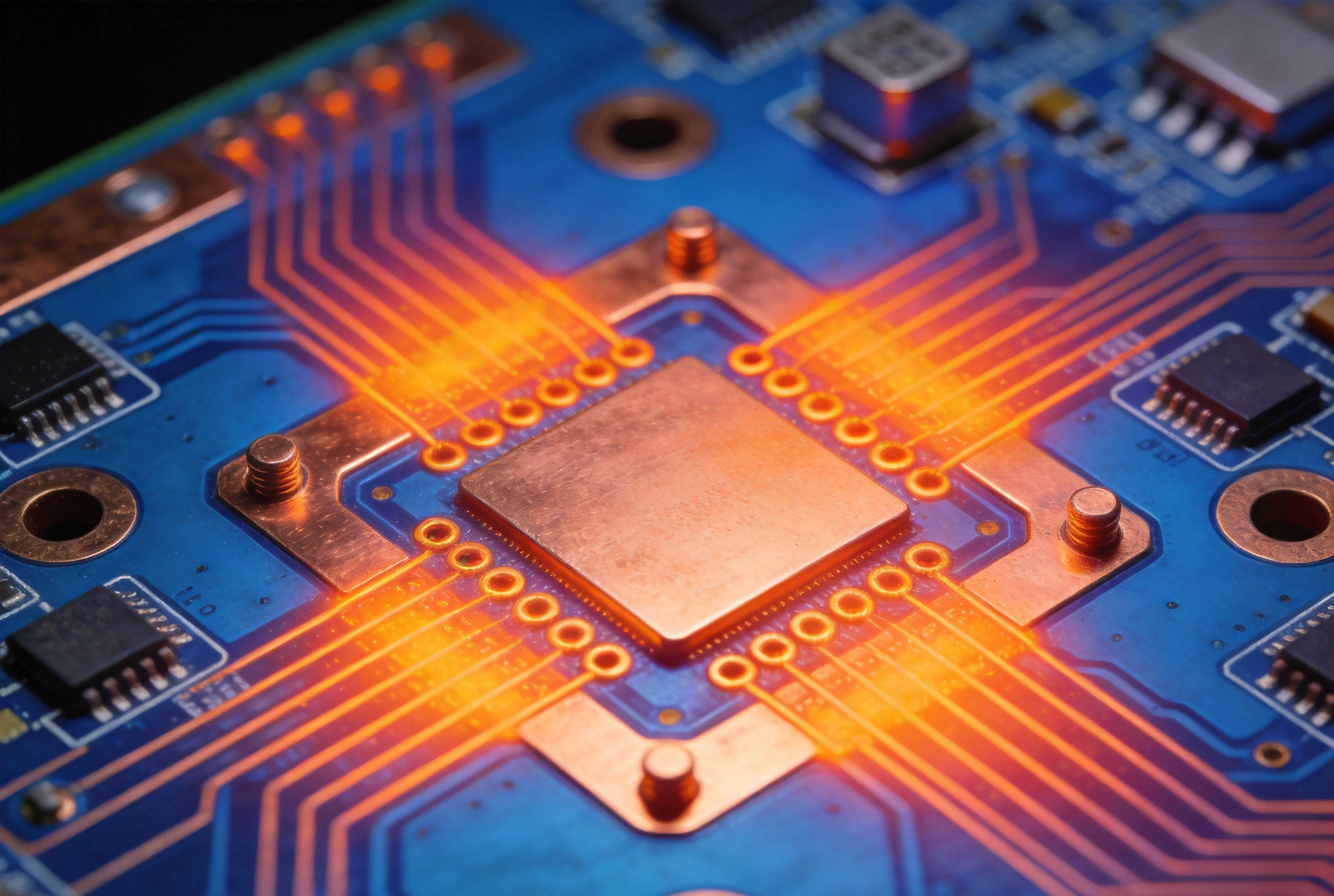
High frequency circuits generate heat through multiple mechanisms that differ from the thermal challenges in low-frequency digital or analog systems. The high-frequency signal propagation itself creates dielectric losses—energy dissipated as heat as the electromagnetic field propagates through the PCB substrate. At gigahertz frequencies, even Dielectric Materials with low loss tangents dissipate meaningful power, particularly in long Transmission Lines or resonant structures where electric field intensity is high.
Component-level heat generation in high-frequency assemblies often concentrates in small areas. Power amplifiers driving high-output RF power can dissipate tens of watts in packages measuring only a few millimeters on each side. RF switches, filters, and other passive components also generate heat through signal losses, though at lower power levels than active devices. This localized heat creates thermal gradients that stress materials and create temperature-dependent performance variations that affect Signal Integrity.
The relationship between temperature and electrical performance adds another layer of complexity. Dielectric Constant of Pcb Materials typically increases with temperature, causing impedance variations that detune matched circuits. Component parameters—gain, noise figure, and switching speed—shift with temperature, creating performance drift that affects system-level behavior. Copper resistance increases with temperature, raising Insertion Loss and potentially creating thermal feedback loops where heating increases losses, which increases heating further. These temperature dependencies mean that thermal management isn't just about preventing failures—it's about maintaining consistent electrical performance.
Dielectric loss tangent quantifies how much energy an insulating material dissipates as heat when subjected to alternating electric fields. At low frequencies, dielectric losses are negligible in most practical circuits. At microwave and Millimeter Wave frequencies, these losses become substantial contributors to total power dissipation. The relationship between frequency, electric field intensity, material loss tangent, and heat generation follows predictable physics, but the practical consequence is that high-frequency PCBs generate heat simply by conducting signals.
The heat generated by dielectric loss distributes throughout the dielectric material, creating a uniform heating effect that raises the overall board temperature. This differs from component heating, which creates localized hot spots. Uniform board heating affects all traces equally, creating temperature-dependent parameter shifts across the entire circuit. The resulting performance variations can be subtle—changes in resonant frequency, slight impedance mismatches, small gain variations—but they accumulate to affect system-level performance, particularly in narrowband applications where tight frequency control is required.
Material selection significantly affects dielectric heating. High-performance Low-loss Materials like Rogers Laminates or specialized Ptfe-based substrates exhibit loss tangents as low as 0.0002-0.0009 at 10 GHz, minimizing dielectric heating. Conventional FR4 materials, with loss tangents around 0.02 at the same frequency, generate 20-100 times more heat from dielectric losses alone. Material selection therefore represents the first and most important thermal management decision for high-frequency designs.
Temperature changes affect high-frequency circuit performance through multiple mechanisms. Understanding these effects helps engineers design thermal management strategies that address not just overheating but also performance stability.
Dielectric Constant temperature coefficient (Dk-Tc) quantifies how much a material's dielectric constant changes with temperature. For many high-frequency laminates, Dk-Tc ranges from +50 to +200 ppm/°C—meaning dielectric constant increases 0.005% to 0.02% for each degree Celsius increase. A 50°C temperature rise therefore changes dielectric constant by 0.25% to 1%, shifting the electrical length of Transmission Lines and detuning resonant circuits. For a 2.4 GHz filter with 1% bandwidth, a 1% dielectric constant shift moves the center frequency by 24 MHz—potentially moving critical signals outside the filter's passband.
Copper conductor resistance increases approximately 0.4% per degree Celsius due to electron scattering mechanisms. A 50°C temperature rise increases trace resistance by approximately 20%, raising Insertion Loss in loss-sensitive circuits. For a 6-inch Microstrip line on FR4 carrying a 5 GHz signal, this resistance increase might add 0.5-1.0 dB of additional loss—significant in applications where loss budgets are measured in tenths of a decibel.
Component performance drift with temperature creates system-level effects that compound PCB-level thermal issues. Power amplifiers lose gain and efficiency at elevated temperatures. Low-noise amplifiers exhibit higher noise figures. Mixers and switches show increased conversion loss and isolation degradation. These component-level effects combined with PCB-level parameter shifts can degrade overall system performance substantially if thermal management doesn't keep temperatures within acceptable ranges.
Effective thermal management requires understanding three fundamental principles: heat generation, heat conduction, and heat dissipation. Heat generation occurs where power is dissipated—through resistive losses in conductors, dielectric losses in substrates, and active power dissipation in components. Heat conduction moves this thermal energy through the PCB structure toward heat dissipation mechanisms—air, chassis, or dedicated heat sinks—that ultimately reject heat to the environment.
The thermal resistance network model provides a useful framework for understanding and analyzing thermal paths. Each material in the assembly contributes thermal resistance proportional to its thickness and inversely proportional to its thermal conductivity. Copper has high thermal conductivity (approximately 400 W/m·K), making it an excellent thermal conductor. FR4 laminate has low thermal conductivity (approximately 0.3 W/m·K), making it a thermal insulator. This dramatic difference means that copper planes and traces form efficient thermal paths while the dielectric material between them creates thermal bottlenecks.
Thermal via arrays are the most common mechanism for overcoming the thermal resistance of dielectric layers. A single plated through-hole provides a vertical copper path through the laminate, conducting heat from surface layers to inner planes or the opposite side of the board. Multiple vias in parallel reduce thermal resistance approximately proportionally—four vias in parallel conduct four times as much heat as one via, assuming equal spacing and plating thickness. Effective thermal via design requires placing vias where heat generation occurs and ensuring the vias connect to copper areas with sufficient thermal mass to absorb and spread the heat.
Thermal via design differs significantly from signal via design. While signal vias require careful placement to minimize discontinuities and maintain Controlled Impedance, thermal vias should be placed wherever they're needed to conduct heat without regard for electrical routing constraints. Large arrays of vias under hot components are common and effective. The key design parameters are via diameter, plating thickness, via pitch, and the total number of vias in the array.
Via diameter affects thermal capacity in two ways. Larger diameter vias have greater cross-sectional copper area, reducing resistance to heat flow. However, larger vias also remove more dielectric material, potentially weakening the board structure and reducing available copper area for signal routing. Practical thermal via diameters typically range from 0.2 mm to 0.3 mm, balancing thermal performance with structural and routing considerations.
Plating thickness directly affects thermal conductance. Standard through-hole plating of 25 microns provides adequate thermal performance for many applications. Heavy copper plating of 50-75 microns reduces thermal resistance substantially and may be necessary for extreme heat dissipation requirements. The plating process must achieve consistent thickness throughout the via barrel—thin spots create thermal bottlenecks that limit overall array performance.
Via pitch determines how densely vias can be packed into the available area under a component. The minimum pitch is limited by via diameter and the minimum webbing required for structural integrity. For 0.25 mm vias, a pitch of 0.5 mm (center-to-center spacing) provides 0.25 mm webbing between vias. This density allows approximately 400 vias per square centimeter under a component—a substantial thermal conducting array for most applications.
Copper planes serve dual purposes in high-frequency PCBs: they provide electrical ground or power reference and they act as thermal spreading plates that distribute heat across the board. Large copper areas absorb thermal energy from concentrated heat sources and spread it over a larger surface area, increasing the effective area available for heat dissipation to the environment.
Ground planes typically occupy substantial area in high-frequency designs, making them natural thermal spreaders. However, the effectiveness of ground planes for thermal spreading depends on how well they're connected to heat sources. Thermal vias that connect hot components directly to the Ground Plane provide efficient thermal transfer. Without these thermal connections, heat must travel through dielectric layers with poor thermal conductivity before reaching the plane, creating thermal resistance that limits spreading effectiveness.
Power planes also contribute to thermal management, particularly in circuits where significant current flows through the plane itself. The I²R losses in power planes generate heat directly in the copper, which spreads through the plane and dissipates to the environment. In high-current RF power amplifiers, the power distribution plane may generate substantial heat, requiring careful thermal analysis to ensure the plane doesn't become a heat source rather than a heat spreader.
Layer stackup design affects thermal spreading capability. Boards with internal copper planes distribute heat more effectively than boards with only surface copper because internal planes provide thermal mass without direct exposure to ambient cooling. However, internal planes require thermal vias to transfer heat from surface layers, adding thermal resistance to the path. The optimal stackup for thermal management balances the thermal benefits of internal planes against the thermal resistance required to access them.
Material choice represents the most fundamental thermal design decision because material properties affect heat generation, heat conduction, and heat dissipation simultaneously. No single material optimizes all thermal parameters—trade-offs are inevitable. Understanding these trade-offs enables informed material selection for specific application requirements.
Standard FR4 laminate exhibits thermal conductivity of approximately 0.3 W/m·K—essentially an insulator from a thermal perspective. Heat must travel through FR4 by conduction only through copper vias and planes, creating thermal bottlenecks that limit heat spreading and dissipation. For high-frequency designs with substantial power dissipation, FR4's poor thermal conductivity often becomes the limiting factor in thermal performance.
High-frequency laminates with improved thermal conductivity address this limitation. Rogers RO4000 series materials achieve thermal conductivity of 0.6-0.8 W/m·K—double to triple that of FR4. Some specialized Ptfe-based laminates reach 1.0 W/m·K or higher. Metal-core PCBs, which use aluminum or copper substrates with dielectric layers, achieve thermal conductivity exceeding 1.5 W/m·K in the through-thickness direction. These material choices significantly improve heat conduction away from hot components, reducing peak temperatures and thermal gradients.
The thermal conductivity improvement comes with cost and processing trade-offs. Metal-core boards require specialized fabrication processes and cannot achieve the same layer counts as laminate-based boards. High-conductivity laminates cost significantly more than standard FR4. The designer must evaluate whether the thermal performance improvement justifies the additional cost and processing complexity.
Heavier copper improves thermal performance by increasing the cross-sectional area available for heat conduction. Standard 1 oz copper (35 microns thickness) provides adequate thermal conduction for many applications. Heavy copper constructions—2 oz (70 microns), 3 oz (105 microns), or heavier—substantially improve heat spreading, particularly in surface traces that must conduct heat laterally to thermal vias.
Heavy copper affects both thermal and electrical performance. The improved thermal conductivity reduces hot spot temperatures and improves reliability. The increased copper cross-section also reduces DC resistance, lowering I²R losses in power distribution traces. However, heavy copper affects high-frequency performance through Skin Effect—current concentrates near the conductor surface at high frequencies, so the center of heavy copper contributes less to conduction than at DC. For thermal purposes, the entire copper thickness contributes, making heavy copper more valuable for thermal management than for high-frequency signal transmission.
Thermal management extends beyond board design into assembly practices and component selection. How components are attached, how the board is mounted in the system, and which components are chosen all affect the overall thermal performance of the assembly.
Choosing components with appropriate thermal characteristics is the first assembly-level thermal decision. Power amplifiers with higher efficiency generate less heat for the same output power. Low-loss passive components—filters, switches, and attenuators—dissipate less power than higher-loss alternatives. Component datasheets typically provide thermal resistance data and maximum junction temperature ratings; using this data during component selection ensures that chosen devices can operate reliably within the intended thermal environment.
Component Placement affects thermal distribution on the board. Grouping high-power components together can create localized hot spots that exceed thermal limits. Spacing heat-generating components across the board distributes the thermal load more evenly, reducing peak temperatures and improving overall reliability. However, spreading components increases trace lengths, potentially degrading high-frequency electrical performance. The optimal placement balances thermal and electrical requirements.
How the PCB mounts in the system affects its ability to dissipate heat. Boards mounted to metal enclosures or chassis can conduct heat directly to the metal, which then dissipates heat to the ambient environment. This conduction path is typically more efficient than convection to air, especially in sealed enclosures with limited airflow. Thermal interface materials between the board and the chassis improve thermal contact by filling microscopic air gaps that would otherwise impede heat transfer.
Heat sinks attached directly to hot components or to the PCB itself provide additional thermal mass and surface area for heat dissipation. For high-power RF devices, metal can packages with exposed thermal tabs connect directly to copper pours or heat sinks through thermal vias. The thermal interface between the device and the heat sink—typically thermal paste or thermally conductive pads—must be applied correctly to minimize thermal resistance. Air bubbles or uneven application create thermal bottlenecks that reduce heat sink effectiveness.
Airflow over the board surface dramatically improves heat dissipation through convection. Natural convection—air movement caused by temperature differences alone—provides baseline cooling. Forced convection using fans increases the convection coefficient by factors of 5-10, dramatically reducing thermal resistance between the board surface and ambient air. In systems where acoustic noise permits, forced air cooling represents one of the most effective and lowest-cost thermal enhancement strategies.
For sealed or enclosed systems where forced air isn't feasible, alternative convection enhancement methods exist. Heat pipes embedded in the chassis transfer heat from hot spots to cooler areas where convection is more effective. Thermoelectric coolers provide active cooling in applications where temperature stability is critical. These approaches add cost and complexity but enable reliable operation in thermally challenging environments.
Designing effective thermal management requires analysis tools to predict temperatures and validation testing to confirm predictions. The combination of simulation and measurement provides confidence that thermal design decisions will produce reliable field performance.
Finite element thermal analysis software predicts temperature distributions in PCB assemblies based on material properties, component power dissipation, boundary conditions, and convection coefficients. These tools enable what-if analysis—evaluating the thermal impact of different via counts, copper plane configurations, and airflow patterns before committing to hardware. Advanced tools couple thermal analysis with electrical analysis, capturing the interdependence between temperature and electrical performance that characterizes high-frequency systems.
Simulation accuracy depends heavily on input data quality. Component power dissipation must be estimated correctly—using typical operating conditions rather than worst-case or idealized values that don't represent real-world operation. Material thermal properties must be accurate for the specific materials used in the design. Boundary conditions—ambient temperature, airflow velocity, and mounting configuration—must reflect the actual operating environment. Simulation with optimistic assumptions produces temperature predictions that prove too low, leading to unexpected thermal issues in fielded products.
Infrared thermal imaging provides direct visualization of temperature distribution on operating PCB assemblies. Handheld IR cameras measure surface temperatures across the board, revealing hot spots that may not be predicted accurately by simulation. For high-frequency assemblies, IR imaging helps identify localized heating from dielectric losses in transmission lines, hot components, and thermal bottlenecks in copper planes or via arrays.
IR imaging limitations must be understood when interpreting results. IR cameras measure surface temperature, not internal component junction temperature. The relationship between surface temperature and junction temperature depends on thermal resistance through the package and Pcb Assembly—data that must be measured or estimated. Additionally, IR cameras cannot measure temperature through metal surfaces—copper planes and heat sinks appear as reflections rather than temperature readings. Despite these limitations, IR thermography provides invaluable insight into actual thermal behavior that complements simulation predictions.
Thermal test vehicles—specialized boards designed specifically for thermal characterization—provide controlled environments for measuring thermal performance. These boards include embedded temperature sensors, precisely defined power dissipation sources, and standardized thermal boundary conditions. By measuring temperatures at multiple points under known power dissipation and environmental conditions, test vehicles characterize the thermal resistance network of the assembly design, providing data that validates simulation models and informs design improvements.
Dielectric loss power dissipation (P_d) is calculated as P_d = V² × ω × C × tan(δ), where V is the RMS voltage across the dielectric, ω is angular frequency (2πf), C is capacitance, and tan(δ) is loss tangent. For transmission lines, the voltage varies along the line, requiring integration over the line length. Simulation tools perform this calculation automatically, but manual estimation is possible for simple cases. A 50-ohm line carrying 10 V RMS at 10 GHz through a dielectric with tan(δ) = 0.02 and C = 100 pF/m dissipates approximately 6.3 W per meter of line length—substantial heat that requires thermal management.
For RF power amplifiers dissipating 5-20 W, thermal via arrays typically use 0.25 mm diameter vias on 0.5-0.75 mm pitch, with 25-50 micron copper plating. Arrays of 20-50 vias under the device provide adequate thermal conduction for most applications. The exact number depends on power dissipation, available board area, and allowable temperature rise. Larger vias (0.3 mm) with heavier plating (50 microns) reduce the required via count but consume more board area. The optimal design balances thermal performance against routing and space constraints.
Thermal vias under transmission lines create impedance discontinuities that can affect signal integrity. A single via under a controlled-impedance line creates a small but measurable discontinuity; arrays of vias create larger discontinuities. For most applications, avoiding thermal vias directly under signal traces is preferable. However, if thermal requirements demand via placement under traces, the via pattern should be symmetric with respect to the trace to maintain balanced impedance, and the number of vias should be minimized while still achieving adequate thermal performance. Alternative approaches place thermal vias adjacent to the trace rather than directly under it, providing thermal benefit while preserving signal integrity.
Ambient temperature sets the baseline for all thermal calculations. A design optimized for 25°C ambient will operate approximately 25°C hotter at 50°C ambient, potentially exceeding temperature limits. High-frequency designs should specify the maximum ambient temperature the product must tolerate and design for thermal performance at that worst-case condition rather than assuming room temperature operation. Military and automotive applications often require operation up to 85°C ambient, which dramatically increases thermal management requirements compared to consumer electronics assuming 25-40°C ambient.
Millimeter wave (30-300 GHz) circuits have similar thermal management requirements to lower frequency Microwave Circuits, with some additional considerations. The smaller wavelengths at millimeter wave allow tighter component spacing, concentrating heat generation in smaller areas. This increases the importance of local thermal management under individual components. Additionally, millimeter wave circuits often use very thin dielectric layers to minimize dielectric loss, which reduces the thermal path thickness and increases thermal resistance. Effective thermal management at millimeter wave frequencies requires even more aggressive use of thermal vias and copper spreading than at lower frequencies.
Thermal management in high-frequency Pcb Assembly is not optional—it's fundamental to achieving reliable performance and predictable field operation. The heat generated by dielectric losses, component power dissipation, and resistive losses accumulates in the PCB structure, and without deliberate thermal management strategies, this heat degrades electrical performance and accelerates material aging. The temperature-dependent nature of high-frequency circuit parameters means that thermal stability is as important as thermal safety—circuits must not only survive temperature but also maintain consistent electrical characteristics across their operating temperature range.
Effective thermal management for high-frequency assemblies combines multiple strategies: material selection that minimizes heat generation, thermal via arrays that conduct heat away from hot spots, copper planes that spread thermal energy, assembly practices that enhance heat dissipation, and validation testing that confirms thermal performance. No single approach solves all thermal challenges—the most robust designs incorporate multiple complementary strategies that address heat generation, conduction, and dissipation throughout the assembly.
The investment in thoughtful thermal management pays dividends throughout the product lifecycle. Boards that operate within specified temperature ranges exhibit more consistent electrical performance, longer operational life, and fewer field failures. In high-frequency applications where performance margins are tight and failure costs are high, these benefits justify the engineering effort required to implement effective thermal management. Understanding the thermal principles described in this article provides the foundation for creating High-frequency Pcb assemblies that deliver reliable performance in demanding real-world environments.
Designing a high-frequency PCB assembly with challenging thermal requirements? Our engineering team specializes in thermal analysis and management for RF, microwave, and millimeter wave applications. Contact us for a thermal design review and optimization recommendations for your specific design.
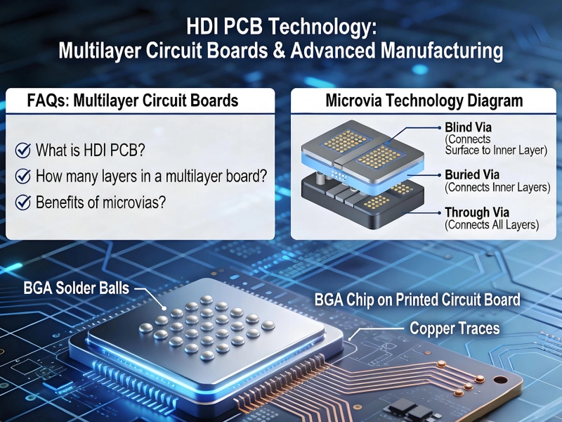
The Benefits of Rapid High Frequency PCB PrototypingMay/29/2026
The Cost of High Frequency PCB Prototyping: What Influences the Price?July/26/2026
Turnkey High Frequency PCB Prototype Services: Streamlining Your Development CycleAugust/06/2026
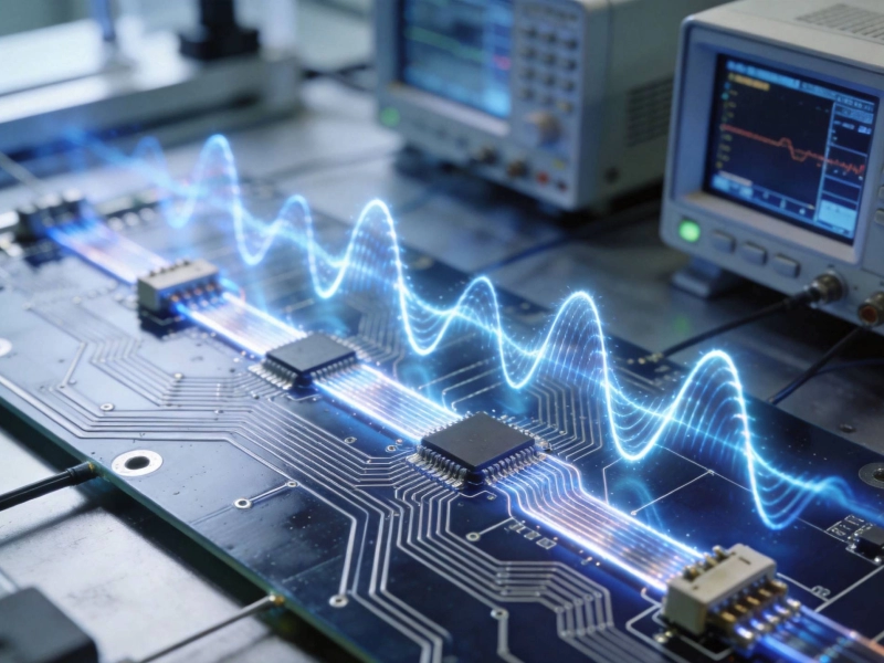
How to Prepare Gerber Files for a Successful High Frequency PCB PrototypeJuly/02/2026
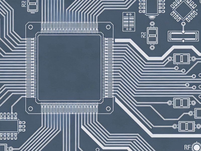
Why Impedance Control is Critical Even in High Frequency PCB PrototypesJuly/14/2026
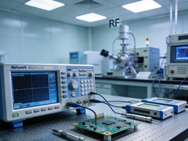
Testing and Validation: Ensuring Your High Frequency PCB Prototype Meets SpecsAugust/15/2026
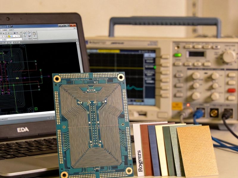
From Design to Reality: A Step-by-Step Guide to Ordering a High Frequency PCB PrototypeSeptember/20/2026
Common Pitfalls to Avoid During Your High Frequency PCB Prototype PhaseJune/18/2026