Open Nav

High frequency printed circuit boards serve applications where Signal Integrity at radio frequencies or microwave frequencies cannot be compromised. From 5G base stations to Automotive Radar systems, from Satellite Communications to Medical Imaging equipment, these specialized boards demand materials and processes far beyond standard Fr-4 production. Understanding what drives the cost of high frequency PCB prototyping helps engineers and project managers budget accurately and make informed trade-offs between performance requirements and cost constraints.
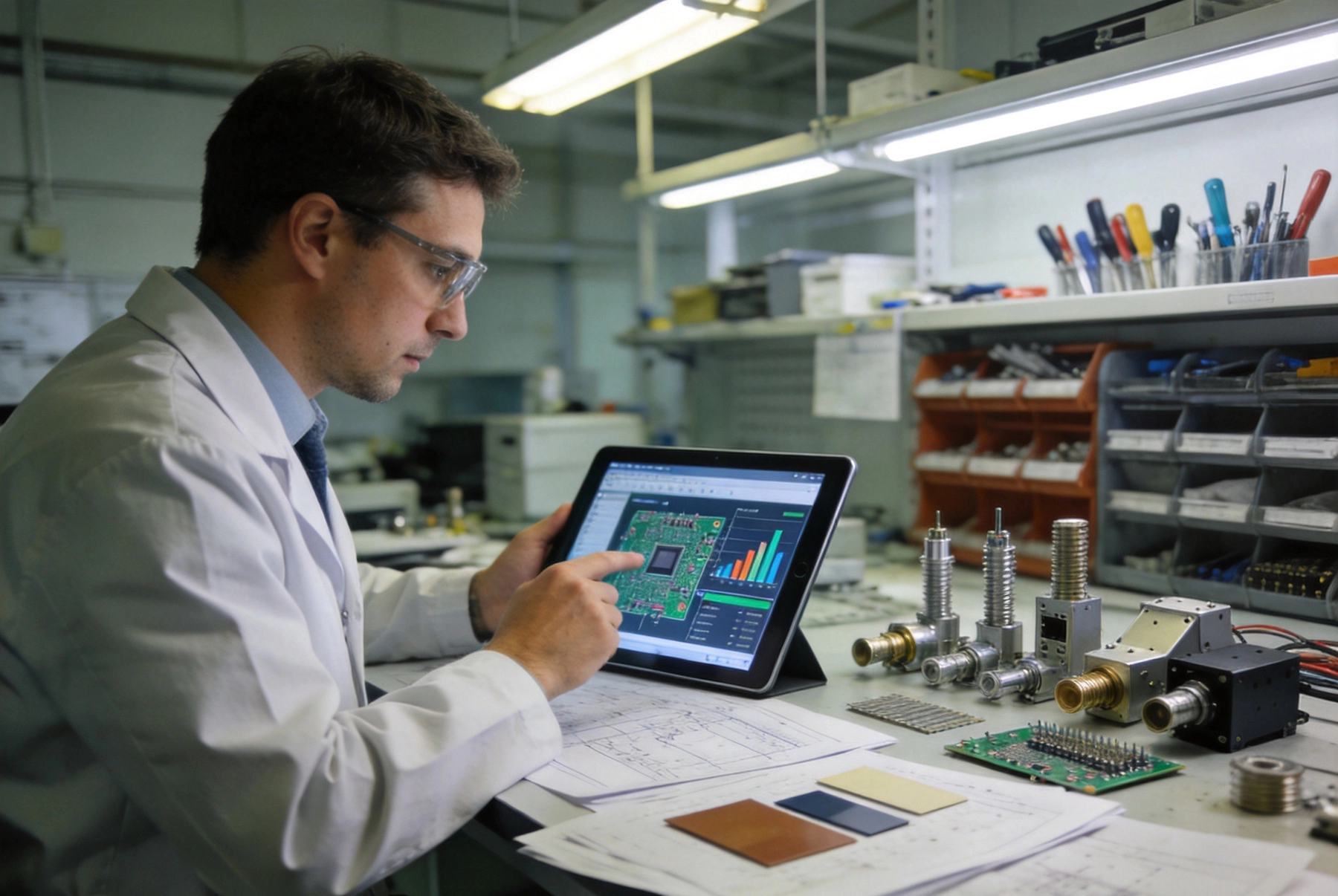
Base material selection represents the most significant cost driver in high frequency PCB prototyping. Standard Fr-4 substrate costs pennies per square inch, while high frequency laminates from manufacturers like Rogers, Taconic, or Isola command prices that can exceed ten times that amount. The hydrocarbon ceramic or Ptfe compositions required for stable dielectric properties at frequency come at a premium that reflects both raw material costs and the specialized manufacturing processes these materials require.
Ptfe-based materials like Rogers RT/duroid series offer exceptional electrical performance but present manufacturing challenges that add to total cost. PTFE's non-polar surface resists standard adhesive bonding, requiring sodium etch treatment or specialized adhesive systems. The material's softness makes it prone to dimensional instability during processing. These handling requirements translate directly into longer cycle times and higher labor costs, even before accounting for the material itself.
Hydrocarbon ceramic blends offer a middle ground, providing good high frequency performance with more forgiving manufacturing characteristics than PTFE. These materials bond readily with standard prepregs and can be processed with conventional equipment, reducing the manufacturing premium. For applications where performance specifications can accommodate slightly higher loss tangent or Dielectric Constant variation, hydrocarbon ceramics often provide the best cost-performance balance.
Larger boards consume more expensive material, though the relationship is not strictly linear. High Frequency Materials often come in standard panel sizes, and inefficient utilization of panel area wastes both material and the manufacturing capacity used to process the board. Panel optimization during layout can significantly impact per-board cost, particularly for prototypes where only single or low quantities are needed.
Multi-layer high frequency boards stack manufacturing complexity geometrically. Each additional layer requires additional lamination cycles, more precise registration, and additional processing steps. Layer count decisions involve trade-offs between routing density, signal isolation, and total cost. Sometimes a board with more layers but simpler stackup achieves lower total cost than a thinner board with fewer layers requiring advanced microvia technology.
Blind and buried vias in high frequency boards compound layer complexity. These structures require sequential lamination steps that interrupt the normal production flow and introduce yield loss. Every additional lamination cycle increases thermal stress on materials already more sensitive to temperature than standard substrates. For prototypes, minimizing via complexity often provides substantial cost reduction without sacrificing performance that prototypes don't require.
High frequency circuits often demand tighter dimensional tolerances than standard PCB production. Trace width control of ±10% may be acceptable for digital circuits, but RF applications requiring specific impedance may need ±5% or tighter. Achieving these tolerances requires Controlled Impedance testing during manufacturing, adding inspection steps and potentially requiring slower, more precise processing equipment.
Dielectric Constant control matters significantly for high frequency performance. Standard FR-4 shows considerable Dk variation across panels and lot-to-lot, typically ±10% or more. High frequency laminates offer tighter control, often ±2% or better, but this control comes at premium pricing and may require additional verification testing. Some manufacturers include Dk testing certificates with material data sheets, while others charge extra for statistical process data or Certificate of Conformance documentation.
Impedance testing on every prototype adds substantial cost, as it requires time-domain reflectometry equipment, specialized test fixtures, and engineering time to interpret results. For prototypes where Impedance Control is critical, testing every board makes sense. For preliminary prototypes where approximate impedance is acceptable, skipping this testing can reduce cost substantially. Understanding which tests are essential versus nice-to-have helps optimize prototype budgets.
Standard 1 oz copper thickness may not suffice for high current RF applications, pushing designs toward heavier copper that adds cost. 2 oz or even 3 oz copper increases material expense and complicates etching, as longer etch times increase risk of undercut and trace width variation. Heavy copper processing requires careful attention to etching parameters and may require additional process controls to maintain tolerance.
Controlled Impedance traces often require plating up to specific thickness, adding another cost layer. Via plating must be controlled precisely for consistent impedance in and out of board, and this typically means slower plating rates and more frequent measurement to achieve target thickness. Via-in-pad and advanced via structures compound this complexity, as fill and cap processes must achieve consistent results across all structures.
Gold plating for connector interfaces or wire bonding adds significant cost beyond standard surface finishes. ENIG (Electroless Nickel Immersion Gold) provides adequate performance for many applications, but RF connector lands may require harder gold over thicker nickel for durability. The choice between ENIG and harder gold systems involves trade-offs between cost, performance, and expected connector mating cycles.
High Frequency Materials often require longer cure times for dielectric stabilization, particularly for PTFE substrates that need careful temperature ramping through multiple stages. These extended thermal cycles consume furnace time that could process more standard boards, creating an opportunity cost that manifests in higher per-board pricing. Planning for prototypes with realistic lead times helps avoid expedite charges that can double or triple costs.
Laser routing and drilling offer precision that mechanical methods cannot match, but equipment time costs more. Microvia formation in high frequency materials requires laser systems capable of cleanly removing dielectric without damaging fine trace geometries. The combination of more expensive equipment and slower processing rates makes laser-based manufacturing substantially more expensive than traditional mechanical routing for prototype quantities.
Edge plating for Grounding or coaxial-like structures requires additional process steps that standard boards don't need. Castellated edges, edge launch connectors, and RF Shielding structures all require specialized handling that adds cost. Prototype boards requiring these features may need custom tooling charges that amortize across production quantities but represent significant upfront investment for one-off prototypes.
Complex geometries with small features require more manufacturing attention and lower yield rates, which translate directly into higher per-prototype cost. Fine line traces below 4 mils, tight spacing between features, and intricate ground pour patterns all increase processing difficulty. What looks simple in a design file may require significant manufacturing expertise to produce reliably.
Controlled impedance structures with multiple reference planes require careful stackup design and modeling. Each impedance-controlled net requires verification, and the interaction between nearby traces can complicate prediction. Designers who specify too many impedance-controlled nets increase inspection burden proportionally. Focusing Impedance Control on truly critical signals while accepting approximate impedance for less sensitive nets reduces cost without sacrificing prototype utility.
Blind and buried via combinations that enable dense routing come at premium cost compared to through-hole-only designs. While these structures make sense for production volumes where routing density reduces layer count, the tooling and process development costs for prototypes often exceed any layer-count savings. For prototypes, simpler via structures typically provide adequate performance at substantially lower cost.
Prototype quantities naturally incur higher per-board cost than production runs, as setup expenses amortize across fewer units. high frequency pcb manufacturing involves significant fixed costs—tooling, material handling, process development—that exist regardless of quantity. A single prototype board may cost five times as much per square inch as the same board in quantities of one thousand.
Expedited turnaround commands premium pricing that can dwarf material costs. High frequency materials typically require longer processing times than standard substrates, and pushing these through faster means overtime labor, dedicated equipment allocation, and potentially accepting lower yields. Rush charges of 50-100% on top of standard pricing are common for fast-turn high frequency prototypes.
Panel efficiency improves with larger quantities, as more boards share the material waste from panel borders and tooling spaces. For prototypes where panel utilization is poor, some manufacturers offer price breaks for two or three boards that fit efficiently on a single panel. This efficiency gain can reduce per-board cost by 30-40% compared to single-board orders.
Electrical testing beyond basic continuity adds cost for every net tested. High frequency designs may require not just opens and shorts testing but full impedance characterization, S-parameter measurement, or time domain reflectometry traces. Each additional test type requires specialized equipment and engineering interpretation time that adds to the invoice.
Quality documentation including Certificate of Conformance, material traceability records, and process travelers adds administrative overhead. For prototypes intended for design verification rather than production deployment, comprehensive documentation may be unnecessary. Understanding which documents are required for the prototype's intended use avoids paying for documentation that won't be reviewed.
Third-party testing or certification for regulatory compliance can exceed prototype board costs by an order of magnitude. UL testing, IPC verification, or customer-specified qualification testing should be planned separately from prototype manufacturing costs. Building certification requirements into prototype specifications from the start avoids discovering late that prototype boards cannot serve as qualification vehicles.
Domestic versus offshore manufacturing involves trade-offs beyond simple labor cost differences. Shipping delays, time zone communication challenges, and intellectual property considerations affect total cost of ownership differently for each project. Prototype boards with urgent timelines may favor domestic suppliers despite higher quoted prices, while schedule-tolerant projects might capture significant savings from overseas production.
Manufacturer specialization matters significantly for high frequency work. Standard PCB shops producing FR-4 boards may quote high frequency work but lack the expertise to handle specialized materials optimally. Shops with dedicated high frequency capabilities and experienced engineering staff may charge more per board but deliver better outcomes with fewer prototypes needed to achieve design verification. The cost of a failed prototype—delays, debugging confusion, redesign iterations—often exceeds the price premium for working with specialists.
Volume commitment agreements can significantly reduce per-prototype cost for companies with ongoing high frequency needs. Manufacturers willing to guarantee future volume often provide substantial prototype subsidies, as they anticipate recovering development costs through production orders. For companies planning multiple high frequency projects, establishing relationships with key suppliers before prototypes are needed creates strategic advantages in cost and scheduling.
Design simplification before prototyping often yields larger cost reductions than negotiation with manufacturers. Reducing layer count, relaxing tolerances where possible, minimizing impedance-controlled nets, and using standard via structures all contribute to lower prototype pricing. Spending engineering time optimizing design typically provides better return than equivalent time spent seeking manufacturer discounts.
Panel utilization optimization through better board placement or size adjustment can reduce material waste significantly. Boards designed for standard panel sizes and efficient nesting yield lower per-board cost. Even small changes like adjusting board dimensions by a few millimeters can improve panel utilization enough to matter for prototype pricing.
Flexible specifications that accept industry-standard tolerances where design margins permit reduce process complexity and yield loss. Demanding tighter tolerances than the application truly requires adds cost without benefit. Working with manufacturers to understand which tolerances are achievable at various price points helps set realistic specifications that achieve prototype objectives within budget.
Not every prototype requires the same performance level as production boards. Preliminary prototypes for concept verification might accept lower performance specifications that enable simpler, cheaper manufacturing. Engineering prototypes for detailed validation should match production specifications more closely, but even these can sometimes use relaxed tolerances for non-critical parameters.
Material substitution with less expensive high frequency substrates may enable acceptable prototype performance at lower cost. Not every application requires the absolute best performing material. Rogers Ro4003c or similar hydrocarbon ceramics provide good high frequency performance at substantially lower cost than Rogers RT/duroid or PTFE materials. Matching material performance to application requirements avoids over-specifying material grade.
Iterative prototyping with increasing complexity allows budget allocation across multiple prototype builds. Starting with simpler, lower-cost boards to verify basic concepts before investing in full-featured high-performance prototypes reduces risk. Each iteration validates assumptions and informs decisions about where additional performance investment makes sense.
Prototype costs represent small fraction of total product lifecycle cost for most electronic systems. A $5,000 prototype that saves one production revision or prevents field failures worth tens of thousands of dollars provides excellent return. Viewing prototype budget decisions in lifecycle context rather than immediate cost minimization often leads to better outcomes.
Production-ready prototypes that serve as qualification vehicles reduce total development cost despite higher initial investment. Boards designed for prototype capability often require redesign before production, adding time and expense. Designing for producibility from the start, even if it means more expensive prototypes, frequently reduces total cost when development and production phases are considered together.
Supplier relationships built during prototyping create strategic value beyond individual project economics. Companies known for clear communication, realistic commitments, and fair dealing develop preferred access to manufacturing capacity and engineering expertise. This relationship value may prove more valuable than price negotiation for companies with ongoing high frequency product development needs.
high frequency pcb prototyping costs reflect a complex interplay of material selection, manufacturing complexity, tolerance requirements, and supplier factors. While the total cost may seem daunting compared to standard Pcb Prototyping, understanding what drives these costs enables informed decision-making that balances performance requirements against budget constraints. Strategic design choices, realistic specification setting, and thoughtful supplier selection can substantially reduce prototype costs without compromising the validation objectives that justify prototyping in the first place.
The key lies in matching manufacturing requirements to actual needs at each development stage. Preliminary prototypes can accept compromises that later-stage prototypes cannot, and structuring development programs to exploit these differences distributes cost across iterations while accumulating the validation information each stage requires. This approach delivers better total outcomes than attempting to achieve production-quality boards in early prototype phases.
Working collaboratively with experienced high frequency manufacturers provides insights that inform design decisions and prevent costly surprises. The best outcomes emerge from partnerships where both parties contribute expertise—designers understanding manufacturing constraints and manufacturers understanding application requirements—to achieve results neither could accomplish alone. This collaborative foundation supports not just individual prototypes but ongoing product development success.
Why do High Frequency Pcb Materials cost so much more than standard FR-4?
High frequency laminates like PTFE composites and hydrocarbon ceramics use specialized raw materials and manufacturing processes that command premium pricing. These materials offer stable electrical properties at radio and microwave frequencies, with tighter dielectric constant control and lower loss tangent than standard substrates. The performance benefits come from both material costs and more challenging processing requirements.
How can I reduce high frequency prototype costs?
Cost reduction strategies include simplifying design complexity, relaxing tolerances where margins allow, using panel-optimized board sizes, specifying standard material grades instead of premium options, and planning realistic lead times to avoid expedite charges. Each design decision to simplify saves multiple times that amount in manufacturing cost.
Is expedited turnaround worth the premium for prototypes?
Expedite charges often equal or exceed base prototype cost, making them worthwhile only when project timelines genuinely require faster delivery. Planning prototypes with adequate lead time typically provides better value. For truly urgent needs, expedited service makes sense, but treating expedite as standard practice wastes budget unnecessarily.
Should I use lower-cost materials for prototypes if production will use premium materials?
Using different materials for prototypes versus production risks validating design decisions with substrates that behave differently at frequency. While preliminary concept prototypes might accept material compromises, engineering prototypes intended for design validation should match production materials closely. Material differences can invalidate prototype conclusions about performance and reliability.
How do I choose between domestic and offshore high frequency manufacturers?
Domestic manufacturers typically offer faster turnaround, easier communication, and potentially better IP protection, at higher per-unit cost. Offshore manufacturers offer lower prices but longer lead times and communication challenges. For prototypes with tight schedules or sensitive IP, domestic sources often provide better value despite higher quoted prices. Schedule-flexible projects with less sensitive technology may benefit from offshore options.
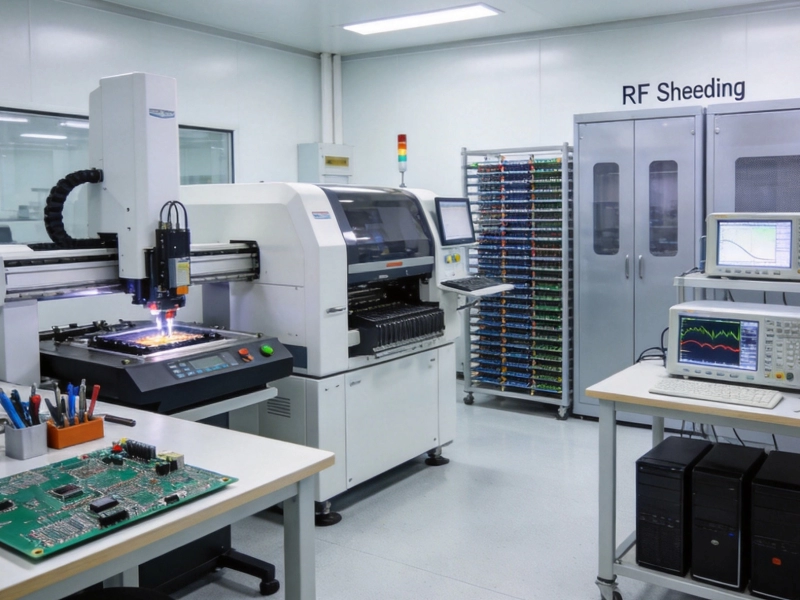
How to Choose the Best High Frequency PCB Prototype Supplier for StartupsSeptember/10/2026
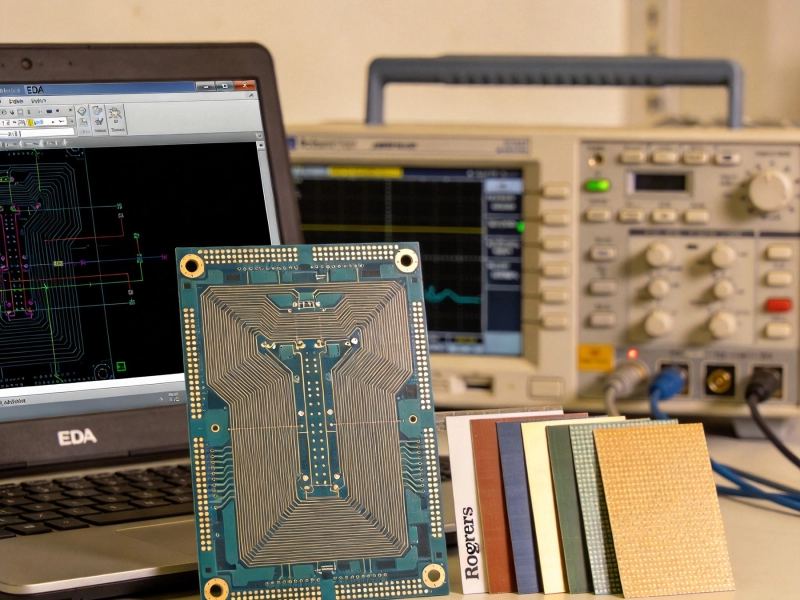
From Design to Reality: A Step-by-Step Guide to Ordering a High Frequency PCB PrototypeSeptember/20/2026
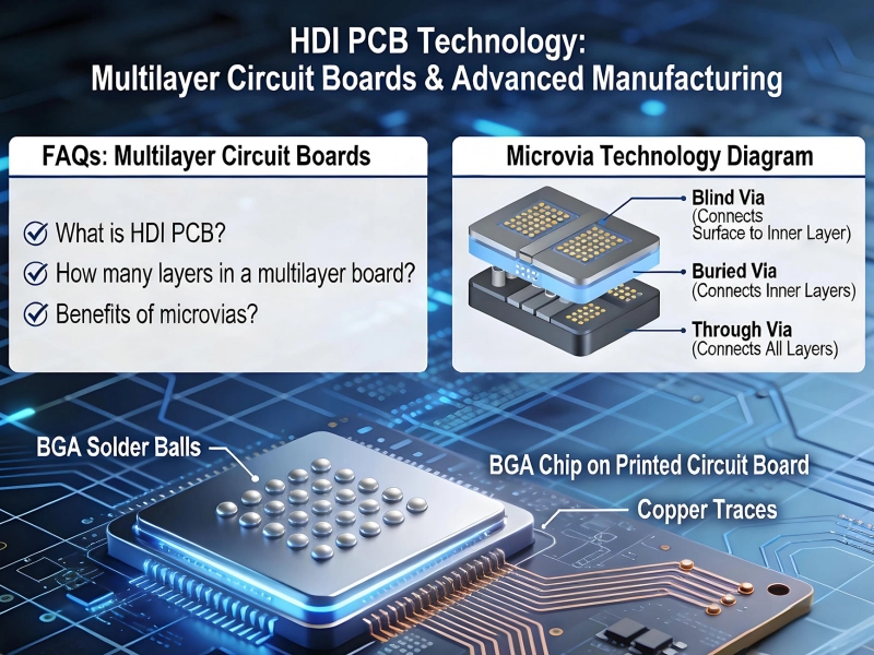
The Benefits of Rapid High Frequency PCB PrototypingMay/29/2026
Common Pitfalls to Avoid During Your High Frequency PCB Prototype PhaseJune/18/2026
How to Prepare Gerber Files for a Successful High Frequency PCB PrototypeJuly/02/2026
Testing and Validation: Ensuring Your High Frequency PCB Prototype Meets SpecsAugust/15/2026
High Frequency PCB Prototype vs. Mass Production: Key Differences in FabricationJune/05/2026

Why Impedance Control is Critical Even in High Frequency PCB PrototypesJuly/14/2026