
Medical imaging technology has revolutionized healthcare, enabling physicians to visualize internal structures and diagnose conditions with unprecedented clarity. Behind these sophisticated systems lies advanced electronics that push the boundaries of high frequency PCB design. From magnetic resonance imaging coils operating at hundreds of megahertz to ultrasound transducers processing signals in the tens of megahertz range, medical imaging equipment demands PCB technology capable of maintaining Signal Integrity at frequencies far beyond typical commercial applications.
The stakes in medical imaging extend beyond equipment performance to encompass direct impacts on patient care. An artifact in an MRI image might mask a tumor. Noise in an ultrasound system might obscure a cardiac abnormality. Inadequate image quality can lead to missed diagnoses, unnecessary procedures, or delayed treatments. high frequency PCB technology must deliver not just adequate performance but the exceptional fidelity that medical diagnosis requires.
This article explores the intersection of high frequency pcb technology and medical imaging applications. Understanding these requirements illuminates both the technical challenges of medical electronics and the advanced manufacturing capabilities that make modern diagnostic equipment possible. From materials selection through manufacturing processes and Quality Assurance, every aspect of high frequency pcb production must meet standards appropriate for life-critical medical applications.
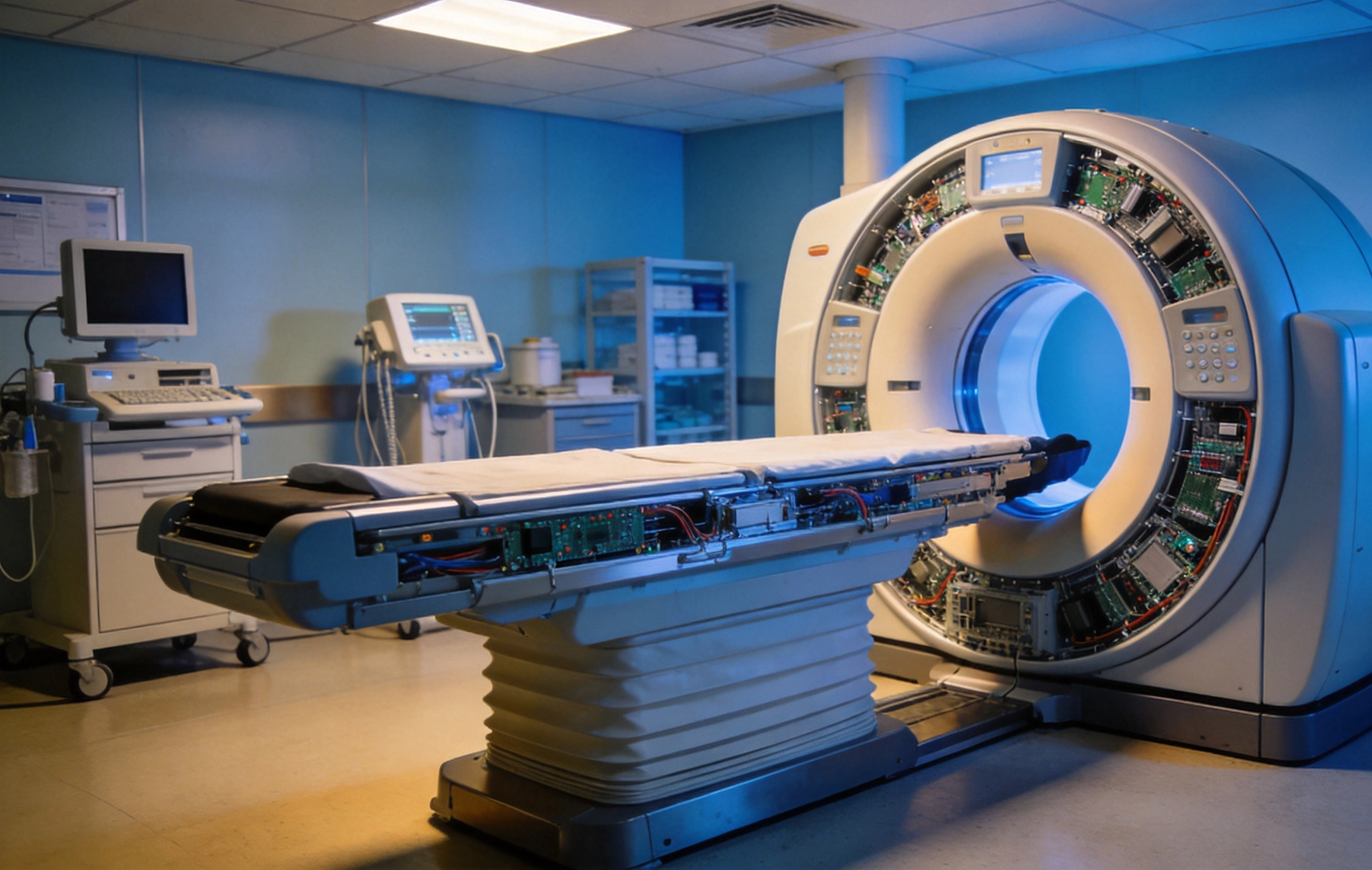
High frequency PCBs differ fundamentally from standard boards in their materials, design practices, and manufacturing requirements. The electrical properties of the substrate—particularly Dielectric Constant and loss tangent—directly influence signal propagation at high frequencies. Medical imaging systems operate across a wide frequency range, from ultrasound frequencies below 20 MHz through MRI systems operating above 300 MHz. Each frequency regime presents distinct challenges that High Frequency Pcb technology must address.
The Dielectric Constant of Pcb Materials determines the velocity of signal propagation and the Characteristic Impedance of Transmission Lines. At high frequencies, materials with stable, consistent dielectric properties are essential for maintaining Signal Integrity. Variations in dielectric constant across a board or between boards create impedance discontinuities that degrade signal quality. Medical imaging demands materials with tight dielectric constant tolerances to ensure consistent image quality across the lifetime of the equipment.
Loss tangent, the measure of energy dissipation in the dielectric material, becomes increasingly important as frequencies rise. High frequency signals lose energy as heat in materials with high loss tangent, reducing signal amplitude and creating noise that degrades image quality. Medical imaging systems amplify extremely weak signals from the human body—sometimes measured in microvolts—and every dB of loss matters. Low-loss Materials are essential for maintaining the signal-to-noise ratios that diagnostic imaging requires.
Ultrasound imaging operates in the frequency range from approximately 1 MHz to over 20 MHz, with higher frequencies providing better resolution for shallow structures and lower frequencies penetrating deeper tissues. The PCB technology for ultrasound systems must handle these moderate frequencies while managing the complex beamforming calculations that create diagnostic images. Phased array transducers with hundreds of elements demand routing densities that challenge even advanced Pcb Manufacturing.
Magnetic resonance imaging employs radiofrequency pulses that interact with hydrogen nuclei in the body. Typical operating frequencies range from 64 MHz for 1.5 Tesla systems to 300 MHz or higher for advanced 7 Tesla research systems. The RF coils that transmit and receive MRI signals must maintain extremely precise phase relationships and minimal losses. Any distortion in the High Frequency Pcb traces that connect to these coils directly affects image quality and potentially patient safety.
Computed tomography and X-ray imaging systems use high frequency electronics for detector array processing and digital conversion. While the imaging physics differs from MRI and ultrasound, the signal processing electronics still demand excellent high frequency performance for rapid data acquisition and image reconstruction. Digital mammography and other specialized imaging modalities have their own frequency requirements that PCB technology must address.
Material selection for medical imaging high frequency PCBs balances electrical performance, reliability, and manufacturing practicality. The frequency requirements of the specific imaging modality determine the acceptable range of material properties. Higher frequencies demand lower loss tangents and more stable dielectric constants. Medical reliability requirements add constraints on thermal stability, moisture resistance, and long-term performance consistency.
Ptfe-based materials represent the highest performance option for demanding high frequency applications. These materials offer the lowest loss tangents available, making them essential for MRI systems operating at the highest frequencies. Ptfe's low dielectric constant provides favorable Impedance Control characteristics. However, PTFE materials present manufacturing challenges including their incompatibility with standard PCB processes, higher costs, and sometimes lower mechanical strength than conventional substrates.
Hydrocarbon ceramic composites offer a balance of electrical performance and manufacturing practicality. These materials achieve loss tangents significantly lower than standard Fr-4 while remaining compatible with modified standard processes. For ultrasound systems and many other medical imaging applications, hydrocarbon ceramics provide the performance necessary at costs and with manufacturing yields acceptable for production volumes.
Medical imaging systems often operate for extended periods, generating heat that must be managed to maintain image quality and system reliability. High frequency circuits are particularly sensitive to thermal effects because temperature changes alter dielectric properties and trace dimensions. Materials with low thermal coefficients of dielectric constant help maintain consistent electrical performance across the operating temperature range.
Heat dissipation from active components in high frequency circuits requires careful Thermal Management. Power amplifiers, low-noise preamplifiers, and digital processing circuits all generate heat that can affect nearby high frequency structures. Thermal design must consider both the impact on PCB electrical performance and the need to maintain component junction temperatures within specifications.
Medical imaging equipment often operates in climate-controlled environments, reducing some thermal challenges. However, the electronics themselves create localized heating that must be managed. Thermal vias, ground planes, and strategic Component Placement all contribute to Thermal Management while maintaining the electrical characteristics that high frequency circuits require.
Magnetic resonance imaging represents perhaps the most demanding application for high frequency PCBs in medical imaging. The RF coils that serve as the antenna for MRI systems must receive extremely weak signals from the body while tolerating the high power pulses used for excitation. Any noise introduced by the electronics directly degrades image quality, and image artifacts can mask pathology or create false positives that lead to unnecessary interventions.
The RF coil interface circuitry operates at frequencies that demand the lowest possible loss and most precise Impedance Control. Trace lengths must be carefully matched to maintain phase relationships across multi-element coil arrays. Even small variations in electrical length can create phase errors that manifest as image artifacts. The exceptional tolerances required for MRI electronics push high frequency Pcb Manufacturing to its limits.
Gradient coil drivers in MRI systems operate at lower frequencies but present their own PCB challenges. These circuits must generate precisely controlled current waveforms with extremely fast transitions. The digital-to-analog conversion and power amplification stages require PCB layouts that minimize parasitic inductances and maintain signal integrity through the entire signal chain. The high currents involved in gradient switching create Electromagnetic Interference that must be contained to prevent image corruption.
MRI environments present unique electromagnetic challenges that influence PCB design. The powerful magnetic fields in MRI systems interact with conductors, creating forces and heating that must be addressed. RF Shielding must contain MRI signals within the imaging volume while preventing external interference from corrupting image data. High frequency PCBs in MRI systems must be designed with these Shielding requirements in mind.
Transmission Lines within MRI electronics must maintain consistent impedance throughout their length. Any impedance discontinuity creates reflections that manifest as ringing or ghosts in the image domain. Careful attention to trace geometry, pad transitions, and via structures minimizes these discontinuities. The exceptional tolerances required for MRI applications often demand specialized manufacturing processes and extensive verification testing.
Grounding and Grounding architecture in MRI PCBs require particular attention. The large differential between the RF frequencies used for imaging and the switching frequencies of digital circuits demands careful isolation. Improper grounding can allow digital noise to couple into sensitive Rf Circuits, degrading image quality. Multi-layer PCBs with carefully designed ground and power planes address these challenges.
Ultrasound imaging systems process signals at frequencies from a few megahertz to over twenty megahertz, with time-of-flight calculations and beamforming algorithms creating diagnostic images from returned echoes. The electronics for ultrasound must handle both the transmission of high-frequency pulses and the sensitive reception and amplification of returning echoes. This combination of high power transmission and low-noise reception presents unique challenges for High Frequency Pcb Design.
The transmit circuitry in ultrasound systems generates high-voltage pulses that excite the piezoelectric transducer elements. These pulses can reach hundreds of volts, creating challenges for component selection and PCB spacing. The rapid edges of these pulses contain high frequency components that require careful routing to prevent radiation and interference with nearby circuits.
Receive circuitry in ultrasound systems must amplify signals measured in microvolts while adding as little noise as possible. The front-end amplifiers and analog-to-digital converters directly determine the dynamic range and sensitivity of the imaging system. PCB design for these circuits must minimize noise coupling, maintain proper grounding, and provide the cleanest possible signal path from transducer to processor.
Modern ultrasound systems use phased array techniques that steer and focus beams electronically across the imaging field. These systems employ large numbers of transducer elements—often 128 or 256 in clinical systems—with dedicated receive channels for each element. The routing density required for these connections pushes PCB technology to its limits, demanding the finest line geometries and most precise impedance control.
Beamforming electronics process signals from all array elements, applying precise time delays that sum constructively at the focal point while canceling elsewhere. The accuracy of these time delays directly affects beam focus and side-lobe levels. Small errors in delay precision can create artifacts that reduce diagnostic utility. High frequency PCB technology must maintain the delay accuracy across all channels and over the temperature ranges encountered in clinical use.
Differential signaling for ultrasound receive channels provides common-mode noise rejection that improves signal quality. The traces carrying these differential signals must maintain consistent spacing and impedance throughout their routing. Any asymmetry in the pair creates common-mode conversion that degrades image quality. Careful attention to pair routing and via transitions maintains signal integrity through the entire receive chain.
Computed tomography systems create cross-sectional images from multiple X-ray projections, requiring high-speed data acquisition and complex reconstruction algorithms. While CT does not operate at radio frequencies like MRI, the detector electronics and digital processing systems still demand High Frequency Pcb Capabilities. The rapid data rates required for clinical CT—often processing millions of samples per second—push PCB bandwidth requirements significantly.
CT detector modules convert X-ray photons to electrical signals through scintillators and photodiodes. The charge integration and digitization circuits that process these signals must operate with exceptional linearity and low noise. The PCB substrates for these modules influence noise performance through dielectric losses and thermal effects on precision analog circuits.
Digital radiography flat panel detectors use amorphous silicon or CMOS sensor arrays with readout electronics that demand high frequency PCB technology. These detectors must capture images with minimal lag while maintaining excellent uniformity across the active area. The electronics that read out and process detector signals benefit from the impedance control and signal routing capabilities that advanced PCBs provide.
Medical imaging systems generate enormous data rates that require sophisticated digital processing. FPGA and ASIC devices with hundreds of pins drive PCB design complexity as signals must be routed to and from these high-density packages. The mixed-signal nature of imaging electronics—with sensitive analog circuits sharing boards with high-speed digital logic—demands careful partitioning and isolation strategies.
SerDes (serializer-deserializer) technology enables the high-speed data transmission necessary for modern imaging systems. These interfaces operate at data rates measured in gigabits per second, requiring Controlled Impedance traces, matched lengths, and excellent signal integrity. The PCBs that carry these high-speed links must meet demanding specifications for loss, skew, and jitter.
Power Delivery for high-speed digital processing circuits presents its own challenges. Modern processors and FPGAs draw current in rapid transients that stress power distribution networks. The simultaneous switching noise from these transients can couple into sensitive analog circuits if not properly contained. Multi-layer PCB structures with dedicated power planes and extensive decoupling address these challenges while maintaining the impedance control that high frequency circuits require.
Designing high frequency PCBs for medical imaging applications requires systematic attention to details that might be less critical in standard electronics. The combination of demanding electrical requirements and life-critical reliability creates design practices that exceed typical commercial standards. Understanding these practices helps appreciate the expertise necessary for medical imaging electronics.
Transmission Line design for medical imaging PCBs must account for the complete signal path from source to destination. Trace geometry must be calculated and controlled for the specific material properties of the chosen substrate. Impedance Matching at every transition—between traces and components, between layers, between connectors—minimizes reflections that corrupt signal quality. The accumulated effect of small discontinuities can significantly impact overall system performance.
Via design requires particular attention because vias create impedance discontinuities that affect high frequency signals. Through-hole vias introduce capacitance at pads and stubs that resonate at certain frequencies. Blind and buried vias eliminate stub effects but add manufacturing complexity. The via strategy must balance electrical performance against cost and manufacturing capability.
Layer assignment for medical imaging PCBs must consider signal types, routing density, and isolation requirements. High frequency signal layers should be adjacent to solid reference planes to provide consistent impedance. Sensitive analog layers benefit from shielding by ground planes that isolate them from noisy digital circuits. Power distribution layers must provide adequate current delivery while maintaining the impedance characteristics that high frequency circuits require.
Trace spacing in medical imaging PCBs must balance density requirements against crosstalk concerns. At high frequencies, crosstalk between adjacent traces can create noise that degrades image quality. Adequate separation, ground guard traces, or routing on orthogonal layers all contribute to crosstalk management. The specific approach depends on signal frequencies, amplitudes, and the signal-to-noise ratios necessary for the application.
Differential pair routing maintains consistent coupling throughout the signal path, maximizing common-mode rejection. The trace width, spacing, and dielectric environment must be precisely controlled to achieve the desired differential impedance. Length matching for timing-critical differential signals must account for the different propagation velocities in the coupled environment.
Manufacturing high frequency PCBs for medical imaging applications demands capabilities beyond standard PCB production. The tight tolerances necessary for consistent impedance, the specialized materials required for low loss, and the reliability standards appropriate for medical devices all create manufacturing challenges. Understanding these capabilities helps appreciate the complexity and cost of medical imaging electronics.
Impedance control tolerances for medical imaging PCBs typically range from ±5% to ±10%, tighter than the ±15% or ±20% acceptable for many commercial applications. Achieving these tolerances requires careful control of trace geometry, dielectric thickness, and material properties. Statistical process control and impedance testing of production panels verify that manufactured boards meet specifications.
High Frequency Pcb Materials often require specialized processing compared to standard Fr-4. PTFE laminates, in particular, require modified handling and processing procedures due to their unique properties. Adhesive systems and bonding processes must be selected to maintain the electrical characteristics of the base material. Not all PCB manufacturers have the capabilities or experience necessary for these specialized processes.
Quality Assurance for medical imaging PCBs encompasses the electrical, mechanical, and reliability characteristics necessary for life-critical applications. Electrical testing verifies continuity, isolation, and impedance across all signals. High-potential testing confirms dielectric integrity under voltage stress. These tests must be documented and retained as part of the traceability record that medical device regulations require.
Impedance testing using time-domain reflectometry verifies that Controlled Impedance traces meet their specifications. Test coupons on production panels enable statistical tracking of impedance capability over time. Any trends indicating process drift trigger investigation and correction before out-of-specification boards reach assembly.
Visual inspection for medical imaging PCBs goes beyond typical acceptance criteria. Surface conditions that might be acceptable for commercial applications may be unacceptable for medical devices where cleanliness and finish affect long-term reliability. Automated optical inspection and, when necessary, manual inspection ensure that boards meet the quality standards appropriate for medical applications.
Medical imaging equipment must operate reliably throughout its service life, often spanning fifteen years or more. This extended service requirement exceeds typical commercial electronics expectations and demands reliability measures throughout design, manufacturing, and qualification. High frequency PCBs for medical imaging must maintain their electrical characteristics over this extended period despite continuous thermal cycling, vibration, and aging effects.
Thermal cycling reliability for medical imaging PCBs must be demonstrated through accelerated life testing. Boards are subjected to temperature extremes that exceed normal operating ranges, with soak periods that stress material interfaces and solder joints. Any degradation in electrical performance—increased loss, impedance shifts, or opens—indicates reliability limitations that must be addressed before production approval.
Electrical reliability testing verifies that high frequency characteristics remain stable over the product lifetime. Extended high-temperature operation accelerates aging mechanisms that might affect dielectric properties. Humidity testing addresses the moisture sensitivity that could affect boards exposed to clinical environments. The combination of these tests provides confidence that medical imaging electronics will perform throughout their service life.
Medical imaging equipment is regulated as a medical device in most jurisdictions, requiring demonstration of safety and effectiveness before market approval. In the United States, the FDA reviews premarket submissions that include design controls, verification and validation testing, and Manufacturing Quality system documentation. Similar requirements exist under the EU Medical Device Regulation and other national frameworks.
The PCB and component qualification for medical imaging devices must follow documented procedures that satisfy regulatory expectations for design controls. Material specifications, process parameters, and acceptance criteria must be established and maintained as controlled documentation. Changes to materials or processes require assessment and potential requalification to ensure that regulatory compliance is maintained.
Supplier Qualification for high frequency PCBs in medical imaging must ensure consistent quality throughout the product lifecycle. Long-term supply agreements and buffer stock of critical components protect against supply disruptions. Supplier audits and periodic requalification maintain confidence that quality standards are maintained over time.
Medical imaging technology continues advancing, driving corresponding evolution in high frequency PCB requirements. Higher field strength MRI systems operating at 7 Tesla and beyond push operating frequencies higher, demanding even lower loss materials and more precise manufacturing. The trend toward portable and point-of-care imaging devices creates pressure for miniaturization while maintaining image quality.
Artificial Intelligence and machine learning are transforming medical imaging, requiring compute densities that challenge PCB technology. Real-time image processing with deep learning algorithms requires FPGAs and processors with ever-increasing pin counts and power dissipation. These demands drive advances in high-density interconnect technology that will benefit medical imaging applications.
Wireless medical devices including ultrasound probes and portable imaging systems create new requirements for high frequency PCBs. The combination of high frequency analog circuits, high-speed digital processing, and wireless transceivers challenges traditional PCB partitioning and design practices. Novel approaches that integrate these diverse functions will shape future high frequency PCB development.
Materials suppliers continue developing new substrates optimized for medical imaging applications. Lower loss tangents, more stable dielectric constants, and improved thermal properties all enable better medical imaging performance. These advances come with tradeoffs in manufacturing complexity and cost that must be balanced against performance benefits.
Embedded component technology promises further miniaturization by integrating passive components within the PCB structure. This approach reduces parasitics and improves high frequency performance while enabling size reduction. While manufacturing challenges remain, embedded technologies will increasingly contribute to medical imaging electronics evolution.
Wide-bandgap semiconductor materials including silicon carbide and gallium nitride enable Power Electronics with improved efficiency and thermal performance. These devices operate at higher temperatures and switching frequencies than traditional silicon, creating both opportunities and challenges for PCB technology. The thermal management and high frequency characteristics of these devices will influence future PCB material and design evolution.
Q: What distinguishes high frequency PCBs for medical imaging from standard high frequency boards?
A: Medical imaging PCBs must satisfy both the demanding electrical requirements of high frequency operation and the reliability standards appropriate for life-critical medical devices. This combination drives stricter material controls, tighter impedance tolerances, more extensive qualification testing, and comprehensive traceability. The cost and complexity are higher than commercial high frequency applications, but the requirements justify these investments.
Q: How do MRI system frequencies affect Pcb Material Selection?
A: Higher field strength MRI systems operate at proportionally higher frequencies, creating greater emphasis on low loss tangent materials. A 3 Tesla MRI operates around 128 MHz, while a 7 Tesla system reaches approximately 300 MHz. The highest field systems often require PTFE-based materials to achieve acceptable loss performance. Lower frequency applications like ultrasound can often use hydrocarbon ceramic materials that offer good performance with more practical manufacturing.
Q: What reliability testing is required for medical imaging PCBs?
A: Reliability testing typically includes thermal cycling to verify resistance to temperature extremes and thermal shock. Vibration testing confirms mechanical robustness for deployment environments. Humidity testing addresses moisture sensitivity. Extended aging tests verify long-term stability of electrical characteristics. Specific test protocols depend on the imaging modality and intended deployment environment.
Q: How does signal integrity affect medical image quality?
A: Signal integrity directly affects image quality through mechanisms including noise introduction, phase distortion, and amplitude errors. In MRI, signal integrity problems create artifacts that can mask pathology or create false positives. In ultrasound, noise degrades dynamic range and resolution. The exceptional signal fidelity necessary for medical diagnosis demands the highest quality high frequency PCB technology.
Q: What is the typical lifespan for medical imaging electronics?
A: Medical imaging equipment is typically expected to remain in clinical service for fifteen to twenty years or longer. This extended service life demands qualification testing and material selection that demonstrate stable performance over these timeframes. The high reliability necessary for medical devices influences all aspects of PCB design and manufacturing.
High frequency PCB technology forms the invisible foundation upon which modern medical imaging systems are built. From the RF coils of MRI scanners to the beamforming electronics of ultrasound systems, the electrical performance of these boards directly determines the quality of diagnostic images that physicians rely upon for patient care. The challenges of high frequency operation in medical applications exceed those of virtually any other domain, demanding materials, manufacturing capabilities, and design expertise at the frontier of PCB technology.
The intersection of high frequency electronics and medical device reliability creates requirements that shape every aspect of PCB production. Materials must offer exceptional electrical properties while maintaining reliability over decades of service. Manufacturing must achieve tolerances that push process capabilities to their limits. Quality assurance must verify not just functionality but the long-term stability that medical devices require. These demands come at costs that reflect the sophistication of the technology and the criticality of its application.
As medical imaging continues advancing toward higher resolutions, faster acquisition, and new modalities, high frequency PCB technology will evolve correspondingly. The engineers who design these systems, the manufacturers who produce the electronics, and the physicians who rely upon the resulting images all depend upon the exceptional capabilities that high frequency PCB technology provides. Understanding this technology illuminates the remarkable achievements of modern medical imaging and the expertise necessary to achieve them.
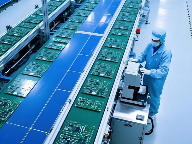
7 Key Factors to Consider When Choosing a High Frequency PCB ManufacturerMay/29/2026
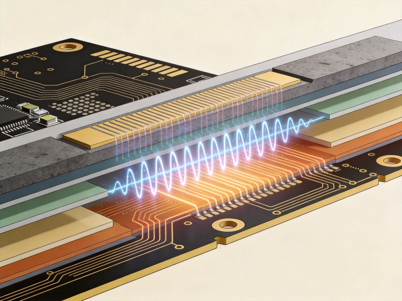
How Dielectric Constant (Dk) and Loss Factor (Df) Affect High Frequency PCB MaterialsJuly/20/2026
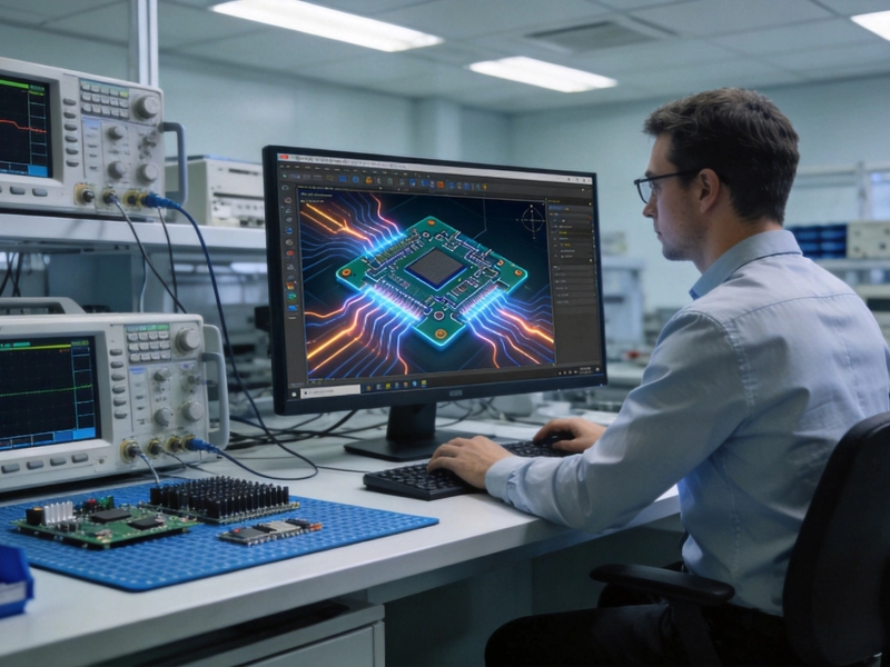
Advanced High Frequency PCB Knowledge: Using Simulation Tools for Better ResultsSeptember/29/2026
High Frequency PCB Applications: Designing for Extreme EnvironmentsOctober/13/2026

Exploring High Frequency PCB Applications in High-Speed Data CentersSeptember/30/2026
Case Study: How the Right High Frequency PCB Manufacturer Solved a Critical EMI IssueSeptember/09/2026

How Our High Frequency PCB Capabilities Support High-Speed Data CentersAugust/08/2026
Advanced High Frequency PCB Fabrication Techniques for Low Loss PerformanceMay/29/2026