
Every time you stream a video, conduct a video conference, or access cloud storage, your data travels through infrastructure built on increasingly demanding electronic foundations. High-speed data centers form the backbone of our connected world, processing petabytes of information daily while maintaining the reliability that modern applications demand. The printed circuit boards inside servers, switches, and routers must perform flawlessly at speeds that would have seemed impossible a decade ago.
Supporting these requirements demands manufacturing capabilities that go far beyond standard PCB production. Our high frequency PCB fabrication combines advanced materials, precision processes, and rigorous quality control to deliver the performance data centers need. Understanding what differentiates high frequency manufacturing from conventional PCB production illuminates why material selection, process control, and testing matter so profoundly for these applications.

Network speeds within data centers have escalated dramatically over recent years. While 10Gbps connections were standard just years ago, current deployments commonly specify 25Gbps, 50Gbps, and even 100Gbps per channel. Front-panel data rates approaching 400Gbps per port are appearing in cutting-edge installations, with 800Gbps implementations on the horizon.
These speed increases aren't merely marketing specifications—they reflect fundamental changes in how electronic signals behave. At 25Gbps NRZ signaling, bandwidth limitations and dispersion effects start degrading signal quality. At 56Gbps PAM4 and beyond, these effects become dominant design constraints that traditional PCB approaches cannot address. Each speed increment demands progressively more sophisticated manufacturing capabilities.
Standard Pcb Materials like conventional Fr-4 were never designed for multi-gigabit signaling. These materials exhibit significant dielectric losses at high frequencies, converting signal energy to heat as it propagates through transmission paths. While this loss might be acceptable for lower-speed signals, it becomes prohibitive at data center speeds where every decibel of loss matters.
Beyond material limitations, standard manufacturing processes introduce variations that compound at high frequencies. Impedance tolerances acceptable for Power Electronics create phase errors that corrupt high-speed signaling. Via structures designed for through-hole mounting create impedance discontinuities that cause reflections and degrade signal quality. High speed data center PCBs require purpose-built manufacturing capabilities.
high frequency PCB manufacturing begins with material selection. Low-loss Dielectric Materials from specialized manufacturers provide the consistent electrical properties that multi-gigabit signaling requires. These materials feature precisely controlled dielectric constants and dissipation factors that minimize signal attenuation across frequency ranges.
Materials like Rogers RT/duroid, Taconic RF laminates, and Panasonic Megtron series offer dissipation factors significantly lower than standard materials. At 10GHz, a Dissipation Factor of 0.002 versus 0.020 represents a tenfold reduction in dielectric loss. This difference directly translates to improved signal reach and reduced error rates in high-speed applications.
High-speed laminate properties extend beyond Dissipation Factor. Coefficient of thermal expansion (CTE) matching between dielectric and conductor affects reliability through temperature cycling. Moisture absorption affects Dielectric Constant stability in humid environments. Glass Transition Temperature (Tg) determines maximum operating temperature before material properties degrade.
Material datasheets provide starting specifications, but understanding how these properties interact under actual operating conditions requires experience and testing. We maintain extensive material characterization data based on manufacturing experience and customer feedback that guides selection for specific applications rather than relying solely on vendor specifications.
Many high-speed PCBs benefit from hybrid material approaches. Critical high-speed signal layers use premium Low-loss Materials while power distribution and lower-speed control layers use standard materials. This hybrid construction balances performance against cost without compromising the signals that matter most.
Hybrid constructions introduce manufacturing complexity that requires careful process control. Different materials have different processing requirements for lamination, drilling, and plating. Managing these differences while maintaining quality across material boundaries demands expertise that distinguishes experienced high-speed manufacturers from those merely claiming high-speed capability.
High-speed signaling requires trace impedance tolerance typically specified at ±10% or tighter. Achieving this tolerance consistently requires manufacturing processes calibrated for Impedance Control rather than merely capable of achieving it on average. We employ statistical process control techniques that maintain impedance within specification across production lots and environmental conditions.
Impedance modeling begins during design, using field solvers that accurately predict impedance based on trace geometry and material properties. These predictions guide manufacturing specifications for trace widths, dielectric thicknesses, and laminate selection. The correlation between modeled and measured impedance validates both design accuracy and manufacturing process consistency.
Via structures create impedance discontinuities that degrade high-speed signals. Multiple techniques address these effects. Back-drilling removes unused via barrel sections that would otherwise create stub resonances. Blind and buried vias eliminate unnecessary penetration through board thickness. Via-in-pad plating fills vias with conductive material that maintains consistent impedance throughout the barrel.
Via aspect ratio—the ratio of board thickness to via diameter—affects manufacturing capability and electrical performance. High-density boards with fine feature capabilities may require smaller vias that present higher impedance discontinuity. Understanding these tradeoffs enables designs that balance density against performance requirements.
Surface finish affects both reliability and high-frequency performance. HASL (hot air solder leveling) creates uneven surfaces inappropriate for fine-pitch components and introduces inductance that affects high-speed signals. ENIG (electroless nickel immersion gold) provides flat surfaces suitable for fine-pitch assembly and maintains stable contact resistance.
For the most demanding applications, specialty finishes like immersion silver or ENEPIG provide specific property combinations. These finishes require controlled processes that maintain consistency across panels and lots. Surface preparation before plating affects adhesion and long-term reliability, requiring process validation for each material-finish combination.
Manufacturing verification of high-speed PCBs requires testing that validates impedance compliance. Time domain reflectometry (Tdr) measures impedance along transmission paths, identifying discontinuities that would affect signal quality. Modern Tdr systems provide resolution sufficient to detect impedance variations over distances measured in millimeters.
Test coupons fabricated alongside production panels provide representative samples for destructive and non-destructive testing. These coupons incorporate Transmission Line structures that undergo the same processes as production boards, validating that process variations do not affect impedance compliance. Coupon testing provides confidence that production boards meet specifications without requiring 100% testing of every trace.
Frequency domain testing using vector network analyzers provides comprehensive characterization of high-speed performance. Insertion Loss measurements verify that signal attenuation stays within budget across operating frequencies. Return loss measurements confirm that Impedance Matching minimizes reflections. Differential pair characterization validates common-mode rejection and differential-to-common-mode conversion.
Network analyzer testing requires calibrated fixtures and experienced operators who understand measurement uncertainty. We maintain metrology-grade calibration systems that provide traceable accuracy, enabling confident assessment of high-speed performance against stringent specifications.
Beyond high-frequency characterization, basic continuity testing verifies that all connections exist as designed. Open circuits, shorts, and wrong net connections represent catastrophic defects that functional testing would detect. High-speed testing cannot replace these fundamental checks—complete test programs include both high-speed performance validation and basic functionality verification.
Isolation testing between adjacent high-speed channels confirms crosstalk levels remain within specification. As data rates increase, crosstalk margins shrink, requiring tighter manufacturing control over trace spacing and coupling characteristics. Automated testing systems provide 100% coverage of isolation specifications across production volumes.
High-speed PCB success requires collaboration between design and manufacturing teams from project inception. Design for Manufacturability (Dfm) reviews identify potential manufacturing challenges before they become production problems. These reviews draw on manufacturing experience to suggest alternatives that achieve performance targets within producible specifications.
Common Dfm findings for high-speed designs include trace width and spacing that challenge manufacturing tolerances, via structures that introduce excessive discontinuity, and reference plane segmentation that creates unexpected coupling paths. Addressing these issues early saves time and cost compared to respinning boards after initial builds fail to meet specifications.
Material selection affects not only electrical performance but also manufacturing capability, reliability, and cost. We consult with customers to understand application requirements and constraints, recommending material-stackup combinations that balance these factors appropriately. Sometimes a slightly higher-loss material with better manufacturing consistency outperforms a theoretically optimal material with marginal process capability.
Stackup design—the arrangement of signal, power, and ground layers—directly affects high-speed performance. Controlled Impedance calculations require accurate modeling of layer thicknesses and dielectric constants. We provide stackup recommendations based on manufacturing capabilities and application requirements, validating calculations against production measurements.
Data center equipment operates in thermal environments that stress electronic reliability. High-speed circuits generate heat that must dissipate to prevent overheating. Thermal design must account for both operating conditions and the thermal resistance of Pcb Materials and constructions.
High-speed materials sometimes trade thermal conductivity for electrical performance. Careful thermal analysis during design ensures that temperature rise stays within component ratings and material limits. Thermal vias, metal core sections, and strategic Component Placement all contribute to Thermal Management in high-speed assemblies.
Data center equipment expectations run to five years or more of continuous operation. This lifespan requires validation that high-speed performance remains stable over time. Thermal cycling, humidity exposure, and vibration testing verify that electrical characteristics do not degrade beyond acceptable limits during intended service life.
Accelerated life testing compresses years of field exposure into laboratory timeframes. These tests validate material selections and manufacturing processes against the demanding conditions that data center environments create. Documentation of reliability validation provides confidence that products will perform throughout their service lives.
Specialty high-speed materials sometimes face longer lead times than standard materials. Some materials require 8-12 weeks for procurement, affecting production schedules for new products. We maintain strategic inventory of common high-speed materials to reduce lead times for customers with established programs.
Material substitutions sometimes become necessary when original materials become unavailable. We coordinate with customers to identify alternative materials with compatible properties, validating that substitutions meet performance requirements. This material management expertise reduces supply chain risk for customers dependent on high-speed material availability.
Transitioning from prototype to volume production challenges many high-speed PCB programs. Prototype quantities might run once monthly while production volumes demand daily output. Manufacturing processes that work at prototype scale may require modification for production efficiency without compromising quality.
We support both prototype and production requirements within the same manufacturing organization. This integration provides continuity from initial development through volume production, maintaining process knowledge that improves yields and reduces qualification time for new programs.
Data center speeds continue increasing toward 112Gbps PAM4 and beyond. These speeds require materials and processes that push current capabilities further. We invest in process development to maintain pace with evolving requirements, qualifying new materials and techniques that enable next-generation data center performance.
Pam4 Signaling—which transmits two bits per symbol instead of one—doubles bandwidth efficiency but introduces signal-to-noise ratio challenges. These challenges cascade through manufacturing requirements, demanding tighter tolerances and more precise process control than NRZ signaling required. Meeting future requirements requires investment in capabilities that address emerging standards today.
Traditional PCB interconnects face fundamental limits as speeds increase. Advanced packaging approaches like embedded components, interposer substrates, and photonic integration offer paths forward when conventional approaches reach limits. These approaches require different manufacturing capabilities than standard Pcb Assembly, demanding investments in new processes and equipment.
We evaluate emerging packaging approaches based on customer requirements and manufacturing feasibility. Some approaches require specialized facilities beyond Pcb Manufacturing; others integrate with existing capabilities through process development. Understanding both the opportunities and limitations of various approaches helps customers make informed architecture decisions.
High frequency PCBs use specialized Low-loss Materials with controlled dielectric properties, tighter manufacturing tolerances for Impedance Control, advanced via structures that minimize discontinuities, and comprehensive testing that validates high-speed performance. Standard PCBs optimized for cost cannot achieve the Signal Integrity that multi-gigabit data rates require.
Our manufacturing capabilities support data rates from 10Gbps through 56Gbps and beyond, depending on material selection and design parameters. Current production volumes support 25Gbps and 56Gbps applications, with 112Gbps capabilities in development for emerging standards.
We offer Rogers Laminates, Panasonic Megtron series, Isola materials, and specialty high-speed composites. Material selection depends on application requirements including frequency range, loss budget, Thermal Management needs, and cost constraints. We recommend specific materials based on your requirements.
Impedance verification uses time domain reflectometry with calibrated equipment, statistical process control to maintain consistency, and test coupon testing alongside production panels. We provide impedance validation reports demonstrating compliance with your specifications.
Typical Controlled Impedance tolerance is ±10%, with tighter tolerances available for demanding applications. Trace width tolerances of ±0.5mil to ±1mil are achievable depending on feature sizes and production volumes. Dielectric thickness tolerances of ±5% to ±10% are typical for high-speed constructions.
Yes, we provide prototype through production capabilities within the same manufacturing organization. This integration provides process continuity and reduces qualification time when transitioning from development to volume production. We support quantities from single prototypes through thousands of units monthly.
High-speed data centers demand Pcb Manufacturing capabilities that exceed what standard production can provide. From specialized low-loss materials through Precision Manufacturing processes and comprehensive testing, every aspect of high frequency pcb production affects the Signal Integrity that data center performance requires.
Supporting data center customers means understanding both the technical requirements and the business pressures they face. Faster development cycles, predictable production costs, and reliable supply chains all contribute to successful product development. We combine technical capability with responsive service to address these broader needs.
As data rates continue increasing and new standards emerge, the demands on PCB manufacturing will only intensify. Our commitment to ongoing capability development ensures that we remain positioned to support next-generation data center requirements. The investments we make today in materials, processes, and expertise prepare us for the challenges that tomorrow's data centers will present.
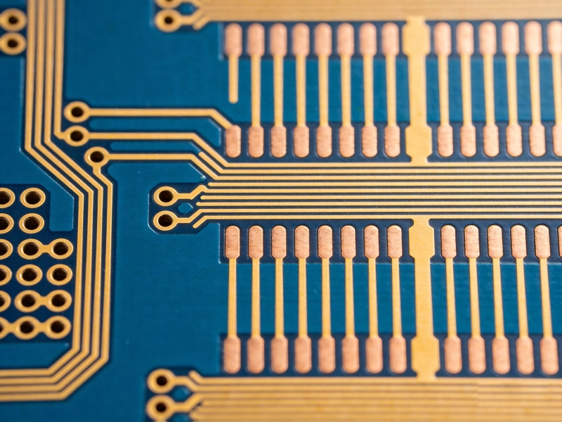
Understanding High Frequency PCB Capabilities: Line Width, Spacing, and Layer CountJune/28/2026
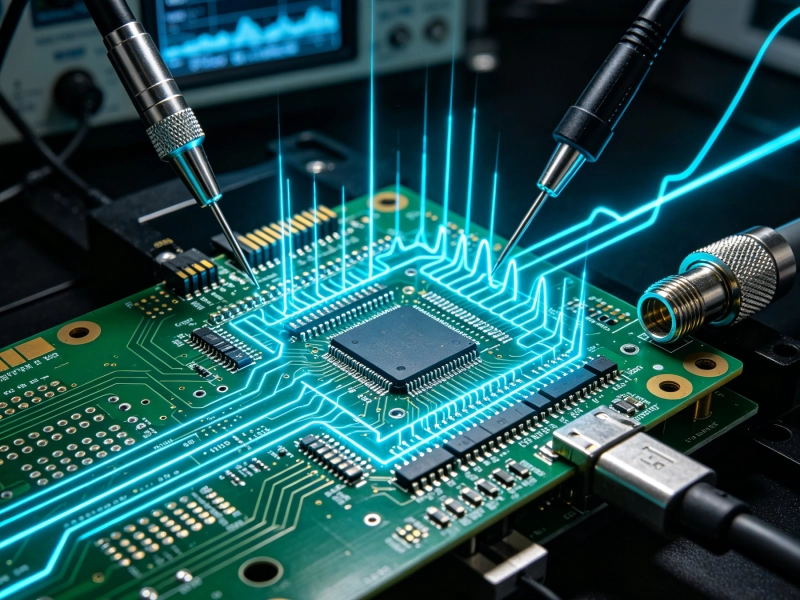
The Importance of Impedance Control in Our High Frequency PCB CapabilitiesSeptember/03/2026
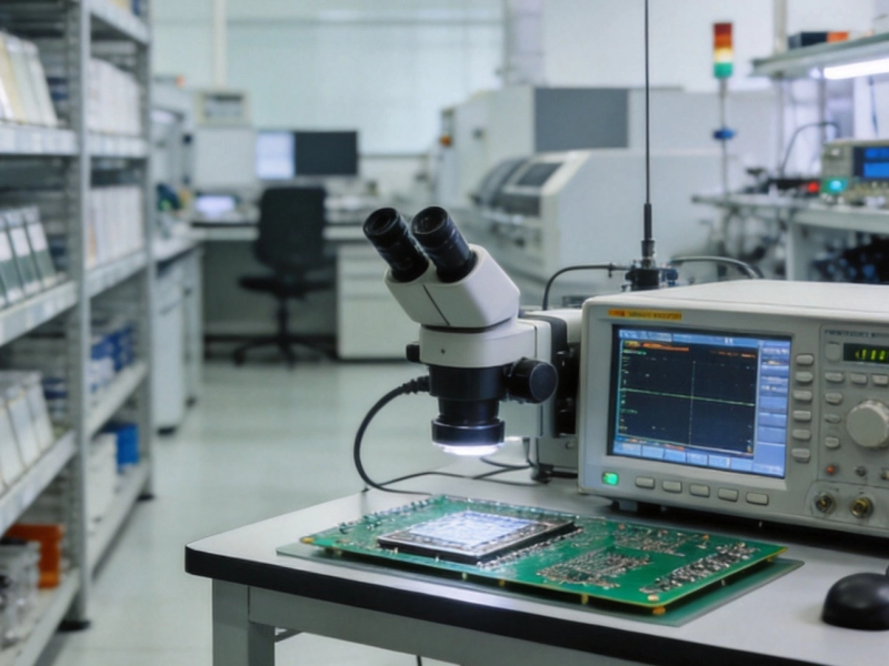
Upgrading Your Supply Chain with Our Expanded High Frequency PCB CapabilitiesOctober/09/2026
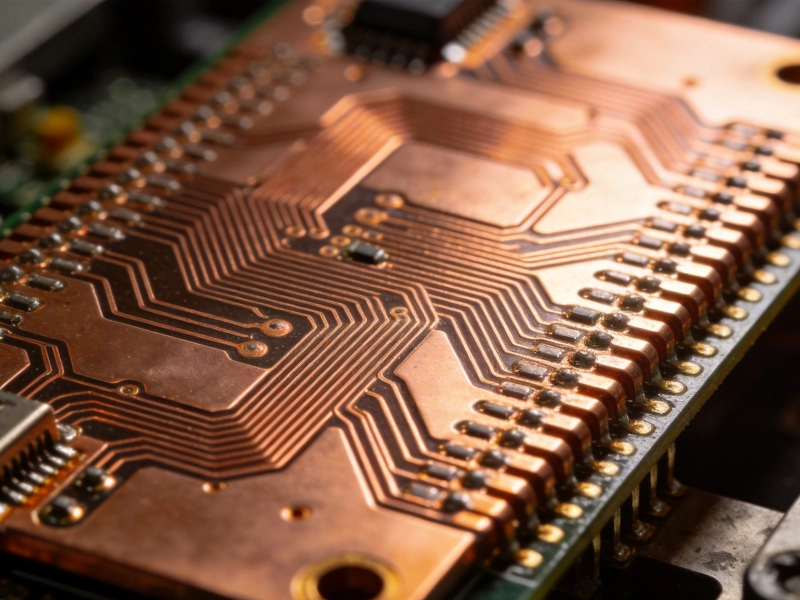
High Frequency PCB Capabilities: Handling Thick Copper and High Power RFSeptember/15/2026
A Deep Dive into High Frequency PCB Capabilities for Millimeter Wave TechSeptember/24/2026
Why Advanced Testing Equipment Defines Top High Frequency PCB CapabilitiesJuly/07/2026

Our Latest High Frequency PCB Capabilities for 6G ResearchMay/29/2026

High Frequency PCB Capabilities for Aerospace and Defense ApplicationsJuly/17/2026