Open Nav
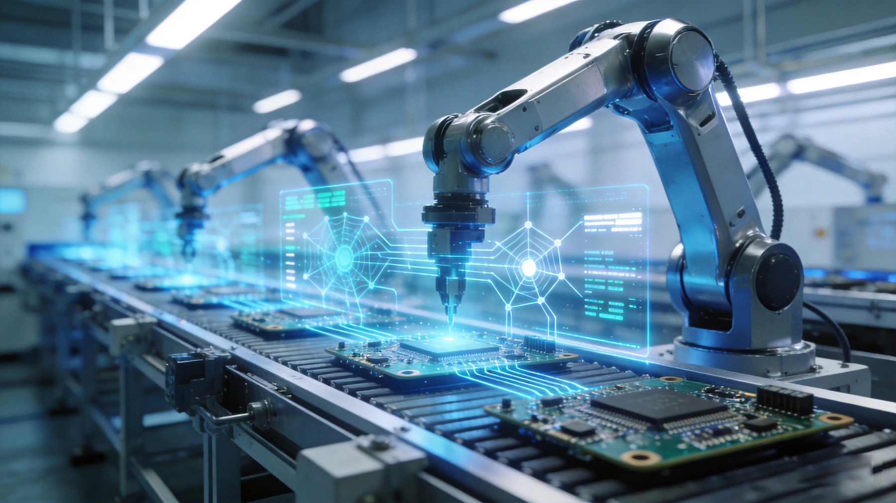
Artificial intelligence has emerged as a transformative force in high-frequency Pcb Manufacturing. As 5G networks, Satellite Communications, and millimeter-wave applications demand increasingly sophisticated circuit boards, traditional manufacturing approaches struggle to meet precision requirements. AI-driven systems now enable manufacturers to achieve unprecedented accuracy while maintaining production efficiency. This article explores how artificial intelligence reshapes every aspect of high-frequency PCB fabrication.
High-frequency printed circuit boards operate at frequencies exceeding 1 GHz, with cutting-edge applications reaching 100 GHz and beyond. At these frequencies, every microscopic imperfection affects Signal Integrity. Trace width variations of just a few microns cause impedance mismatches. Subtle dielectric inconsistencies create Signal Loss. Even minor plating thickness variations degrade performance.
Traditional manufacturing relies on statistical process control and human inspection. These methods cannot detect the subtle defects that impact high-frequency performance. AI systems analyze vast datasets, identifying patterns invisible to human operators. Machine learning algorithms predict process drift before defects occur. Computer vision systems inspect boards with micron-level precision at production speeds.
The economic stakes justify AI investment. A single high-frequency PCB for 5G base stations or radar systems may cost thousands of dollars. Rework expenses multiply when defects escape detection. AI-powered quality assurance pays for itself through yield improvements and reduced field failures.
High-frequency PCB design involves complex trade-offs between Signal Integrity, thermal management, and manufacturability. AI-powered design tools accelerate optimization while improving outcomes.
Controlled Impedance traces require precise width calculations based on dielectric thickness, copper weight, and material properties. AI systems automatically calculate optimal trace geometries for target impedances. They account for manufacturing variations, ensuring designs remain within specification across production tolerances.
Advanced algorithms optimize layer stackups for minimal Signal Loss and crosstalk. They simulate electromagnetic behavior across frequency ranges, identifying potential resonance issues before fabrication. Design rule checks powered by machine learning catch subtle errors that traditional DRC tools miss.
High-frequency circuits generate significant heat. AI systems model thermal behavior during layout, recommending Component Placement and copper distribution for optimal heat dissipation. They balance thermal performance against signal integrity requirements, finding solutions human designers might overlook.
Predictive thermal modeling identifies hotspots before prototyping. Manufacturers avoid costly redesign cycles and reduce time-to-market for complex high-frequency products.
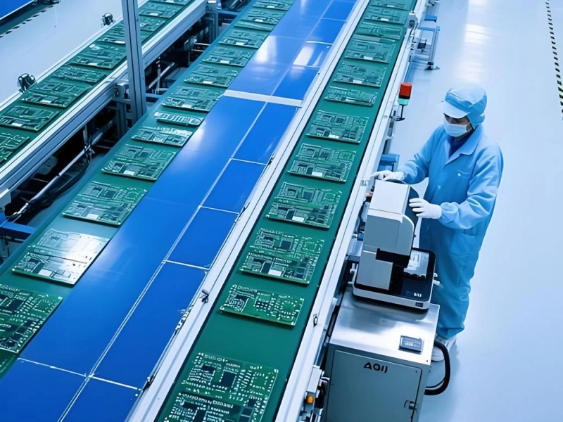
High-frequency PCB fabrication involves dozens of process steps, each affecting final performance. AI systems monitor and optimize these processes in real-time.
Trace geometry directly impacts high-frequency performance. AI-powered etching systems analyze in-process measurements, adjusting etch parameters to maintain tight tolerances. Machine learning models predict etch behavior based on cumulative production data, compensating for bath chemistry variations and panel loading effects.
Closed-loop control maintains trace width consistency within ±5 microns. This precision proves essential for high-frequency applications where Impedance Control determines product functionality.
Copper plating thickness affects both conductivity and signal loss. AI systems monitor plating bath parameters, current distribution, and deposition rates. They adjust process parameters to achieve uniform thickness across complex board geometries.
Predictive models identify when plating chemistry requires replenishment, preventing out-of-specification deposits. This proactive approach reduces scrap and improves first-pass yield.
High-frequency multilayer boards require thousands of precisely positioned vias. AI-enhanced drilling machines compensate for mechanical drift, temperature effects, and material variations. Real-time position correction maintains via placement accuracy within ±25 microns.
Machine learning algorithms optimize drilling sequences to minimize tool wear and maximize positional accuracy. They predict drill bit life, scheduling replacements before quality degradation occurs.
High-frequency PCBs cannot tolerate the defects acceptable in lower-frequency applications. AI-powered automated optical inspection (AOI) systems detect subtle imperfections that threaten performance.
Deep learning models trained on millions of board images recognize defect patterns invisible to rule-based inspection systems. They distinguish between cosmetic anomalies and functional defects, reducing false-positive rates that plague traditional AOI.
Advanced systems inspect inner layers before lamination, preventing buried defects that escape final testing. They measure trace geometries with sub-micron precision, ensuring Impedance Control throughout fabrication.
AI inspection extends beyond visual defects. Some systems analyze copper grain structure, identifying metallurgical issues that affect high-frequency performance. Others detect dielectric contamination that could alter material properties.
Reactive quality control inspects finished boards, scrapping defective products. AI enables predictive quality management, preventing defects before they occur.
Machine learning models analyze historical production data, identifying parameter combinations that produce optimal results. They continuously refine process recipes based on incoming quality data, automatically adapting to material lot variations and equipment drift.
These systems detect subtle correlations between process variables and final performance. They might discover that morning-shift humidity affects Dielectric Constant, or that specific material lots require adjusted etch times.
AI monitors process data streams in real-time, flagging anomalies that precede quality issues. A slight pressure variation in lamination, a minor temperature fluctuation in reflow, or an atypical chemical concentration might indicate impending problems.
Early warning systems alert operators to investigate before defects occur. Some facilities implement automatic process holds when AI systems detect conditions outside historical norms.
Verifying high-frequency PCB performance requires sophisticated testing. AI enhances both test development and execution.
AI systems generate test patterns optimized for specific board designs. They identify critical test points based on signal path analysis, ensuring comprehensive coverage without excessive test time.
Machine learning models predict which test patterns most effectively detect particular defect types. They prioritize tests based on historical failure modes, maximizing defect detection efficiency.
Vector network analyzers generate massive datasets characterizing high-frequency performance. AI algorithms analyze S-parameters, identifying subtle performance variations that indicate manufacturing issues.
Pattern recognition systems compare measured responses against golden references, flagging deviations that might affect system performance. They distinguish between acceptable manufacturing variation and genuine defects requiring rework.
High-frequency PCB performance depends critically on material properties. AI systems optimize material selection and track supply chain quality.
Machine learning models predict material performance based on supplier data, lot characteristics, and historical results. They recommend optimal material choices for specific applications, balancing performance, cost, and availability.
Blockchain-integrated AI systems trace materials from supplier through fabrication, enabling rapid root-cause analysis when issues arise. They identify problematic material lots before they contaminate production.
Despite impressive capabilities, AI systems face limitations in high-frequency Pcb Manufacturing.
Training data quality determines AI performance. Insufficient or biased data produces unreliable models. High-mix, low-volume facilities may lack adequate data for effective machine learning.
AI systems require significant computational resources. Real-time process control demands powerful edge computing infrastructure. Smaller manufacturers may struggle with implementation costs.
Interpreting AI decisions remains challenging. Black-box models may recommend parameter changes without clear explanations. Engineers need transparency to trust and validate AI recommendations.
High-frequency applications continue pushing frequency boundaries. AI models trained on 10 GHz applications may not generalize to 100 GHz designs. Continuous retraining and validation prove essential.
Emerging technologies promise even greater AI integration. Digital twin systems simulate entire manufacturing processes, enabling virtual optimization before physical production. AI-powered robots handle delicate high-frequency materials with superhuman precision and consistency.
Generative AI may eventually design complete high-frequency PCBs from specification documents. Systems could autonomously generate layouts, select materials, and optimize manufacturing processes without human intervention.
Edge AI brings intelligence directly to manufacturing equipment, enabling microsecond-level process adjustments. 5G connectivity supports real-time collaboration between distributed AI systems across global manufacturing networks.
Artificial intelligence has become indispensable in high-frequency PCB manufacturing. From design optimization through process control to final inspection, AI systems enable the precision and consistency that modern applications demand. Manufacturers embracing AI achieve higher yields, better performance, and faster time-to-market.
The technology continues evolving rapidly. Facilities investing in AI infrastructure today position themselves for tomorrow's competitive landscape. As 6G, advanced radar, and Satellite Communications push frequency requirements ever higher, AI-powered manufacturing will prove essential for success.
For electronics manufacturers navigating high-frequency PCB production, AI adoption is no longer optional—it is a strategic imperative that determines market position and technical capability.
Quality and Cost Analysis of High-Frequency Printed Circuit Board Manufacturers in China and the WestJune/04/2026
7 Key Factors to Consider When Choosing a High Frequency PCB ManufacturerMay/29/2026

Why Certifications Matter: IATF16949 and ISO Standards for Your High Frequency PCB ManufacturerJune/17/2026
Top High Frequency PCB Applications in the 5G and Telecommunications IndustryMay/29/2026
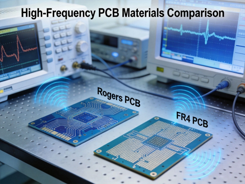
Rogers vs. FR4: Choosing the Right High Frequency PCB MaterialsJune/12/2026
The Challenges of High Frequency PCB Assembly: Handling Sensitive ComponentsMay/29/2026
Common Pitfalls to Avoid During Your High Frequency PCB Prototype PhaseJune/18/2026
Advanced High Frequency PCB Fabrication Techniques for Low Loss PerformanceMay/29/2026