Open Nav
High Frequency Pcb Prototyping demands precision that regular PCB design simply doesn't require. When your signals operate in the gigahertz range, every millimeter of trace geometry, every choice of laminate material, and every manufacturing tolerance becomes critical. Engineers who successfully navigate high frequency prototype development share one common trait: they understand where others fail and plan accordingly. Your next RF or microwave project can benefit enormously from learning from the mistakes that routinely derail high frequency prototypes.
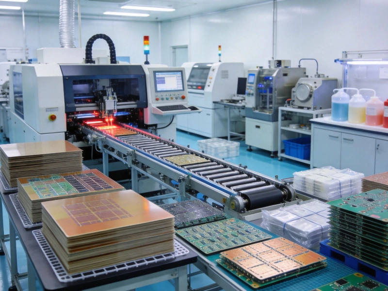
Working with Chinese manufacturers on high frequency prototypes introduces additional complexity. Not all facilities have the equipment, expertise, or quality systems needed for precision RF work. Many factories that excel at standard digital PCB assembly struggle with the tight tolerances that microwave circuits demand. Understanding these challenges before you commit to production prevents the heartbreak of prototypes that work perfectly in your lab but fail consistently when manufactured at scale in Shenzhen or similar manufacturing hubs.
This guide walks you through the most significant pitfalls in High Frequency Pcb Prototyping. Some are purely technical; others involve the human and procedural aspects of working with contract manufacturers. All of them have ended promising projects and frustrated engineering teams. Your goal: avoid these traps by understanding them thoroughly.
The foundation of any High Frequency Pcb is its substrate material. Many engineers default to FR-4 without considering the electrical consequences. At frequencies above 1 GHz, FR-4's Dielectric Constant variation— typically 4.2 to 4.8 with poor tolerance— creates unacceptable impedance uncertainty. Your calculated trace widths may deliver 50 ohms in simulation but deviate significantly in the manufactured board.
High frequency laminates like Rogers RT/duroid, Taconic RF substrates, and Isola IGET offer much tighter Dielectric Constant tolerances, typically ±1% or better. These materials cost more, but they provide the predictability your design needs. Chinese factories have varying库存 and experience with these materials. Some specialize in Rogers and Taconic products; others rarely work with anything beyond standard FR-4. Know your manufacturer's capabilities before specifying materials.
Datasheet dielectric constants represent nominal values, but actual performance varies with frequency, temperature, and humidity. For critical applications, request material characterization data from your laminate supplier. Many high frequency laminate manufacturers provide measured data sheets showing dielectric constant at specific frequencies— information that dramatically improves your modeling accuracy. Without this data, your simulations rest on assumptions that may not hold in the real world.
Impedance Control in high frequency PCBs is not optional— it's mandatory. But many engineers specify Impedance Control without adequately considering the tolerances involved. A ±10% impedance tolerance may sound acceptable until you calculate what it means for your system performance. At 5 GHz, a 10% impedance variation creates significant signal reflection and return loss problems.
Manufacturing tolerances for Controlled Impedance traces depend on the Pcb Manufacturer and their processes. Chinese factories capable of Controlled Impedance typically guarantee ±7% to ±10% on standard lines. Tighter tolerances— ±5% or ±3%— require specialized processing and cost more. Specify your actual tolerance requirement, not just "impedance controlled." If your design needs ±5%, say so explicitly and confirm your manufacturer can deliver it.
Trace width and thickness variations drive impedance errors. Etching processes naturally create some trace width variation, typically ±0.5 mils to ±1 mil depending on the manufacturer. For controlled impedance lines, this variation must be characterized and compensated. Your Chinese factory should provide impedance test coupons on each production panel— insist on this even for prototypes. These coupons verify that the manufacturing process delivered what your design requires.
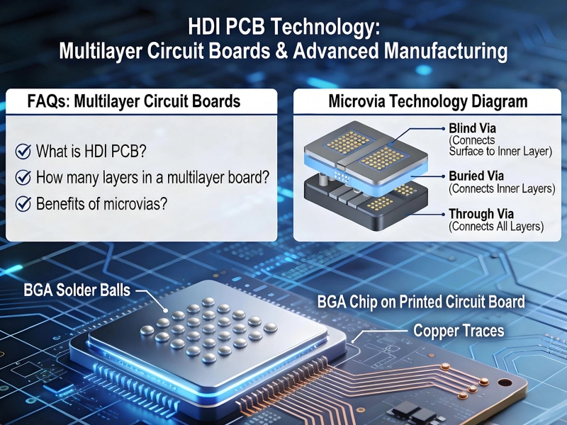
Vias in high frequency circuits introduce discontinuities that can devastate Signal Integrity. The parasitic inductance and capacitance of vias create impedance mismatches, resonance effects, and radiation that degrade circuit performance. Yet vias remain necessary for layer changes in multi-layer designs. Understanding and managing via effects separates successful high frequency designs from disappointing prototypes.
Through vias at microwave frequencies behave as transmission line stubs that resonate at specific frequencies. An unterminated via stub acts as a quarter-wave resonator, creating unwanted peaks in S-parameters at frequencies determined by the stub length. For frequencies where stub resonance falls within your operating band, back-drilling or blind/buried vias become necessary. Many Chinese factories now offer back-drilling services— confirm capability and pricing before you need it.
Via transitions between layers also create capacitive loading. The antipad— the clearance hole around the via through the reference plane— determines this capacitance. Small antipads reduce parasitic capacitance but increase manufacturing difficulty and cost. Your design must balance electrical performance against manufacturing feasibility. Consult with your Chinese prototype house early in the design phase; they can identify problematic via structures before you receive prototypes that fail to meet expectations.
PCB surface finishes affect high frequency performance more than most engineers realize. HASL (Hot Air Solder Leveling) creates uneven surfaces with unpredictable thickness variation— terrible for high frequency signals. ENIG (Electroless Nickel Immersion Gold) provides flat surfaces but introduces additional conductive layers with their own conductivity characteristics. OSP (Organic Solderability Preservative) offers excellentplanarity but minimal protection for extended periods.
For microwave circuits, gold plating thickness matters critically. The skin depth at high frequencies means signals propagate primarily on conductor surfaces. At 10 GHz, skin depth in copper is approximately 0.8 micrometers. If your gold plating is 0.05 micrometers over 0.5 ounce copper, most of your signal still travels in copper. But thicker gold layers— sometimes specified for durability— can introduce additional loss if not properly applied. Validate that your surface finish specification matches your frequency requirements.
Impedance test results vary with surface finish because the effective dielectric constant changes with the plating structure. When you specify controlled impedance, confirm that your manufacturer measures impedance after the final surface finish is applied, not before. Some factories test impedance on raw boards; surface finish then changes the effective impedance by a few percent. This gap between test conditions and actual usage explains why some prototypes pass impedance tests but systems fail in integration testing.
High Frequency Pcb stack-up specification requires attention to detail that many engineers underestimate. The layer structure— dielectric thicknesses, copper weights, prepreg types— directly determines trace geometries needed for target impedances. Incomplete or ambiguous stack-up specifications guarantee prototype failures that consume time and budget.
Each dielectric layer needs specification by material type, thickness, and tolerance. "Core 0.8mm" is not adequate; "1080 prepreg, 0.095mm nominal, ±10% tolerance" communicates actual requirements. Chinese manufacturers accustomed to digital designs may need explicit guidance on what dielectric tolerance their process can achieve versus what your design requires. Misaligned expectations here create prototypes that don't match simulations.
Cross-section drawings should accompany your stack-up specification. Many high frequency design errors stem from misunderstanding how layers stack relative to each other. A reference plane on layer 2 affects traces on layer 1 differently than a reference plane on layer 3. Your stack-up drawing should clearly identify which layers serve as reference planes for which signal layers, and at what distance. Without this clarity, your manufacturer builds what they think you need rather than what you actually specified.
Design for Manufacturability in high frequency PCBs extends far beyond standard Dfm checks. RF structures likecouplers, filters, and antenna elements have manufacturing sensitivities that regular PCB design doesn't encounter. What looks perfectly reasonable in your layout tool may be impossible or extremely expensive to manufacture consistently.
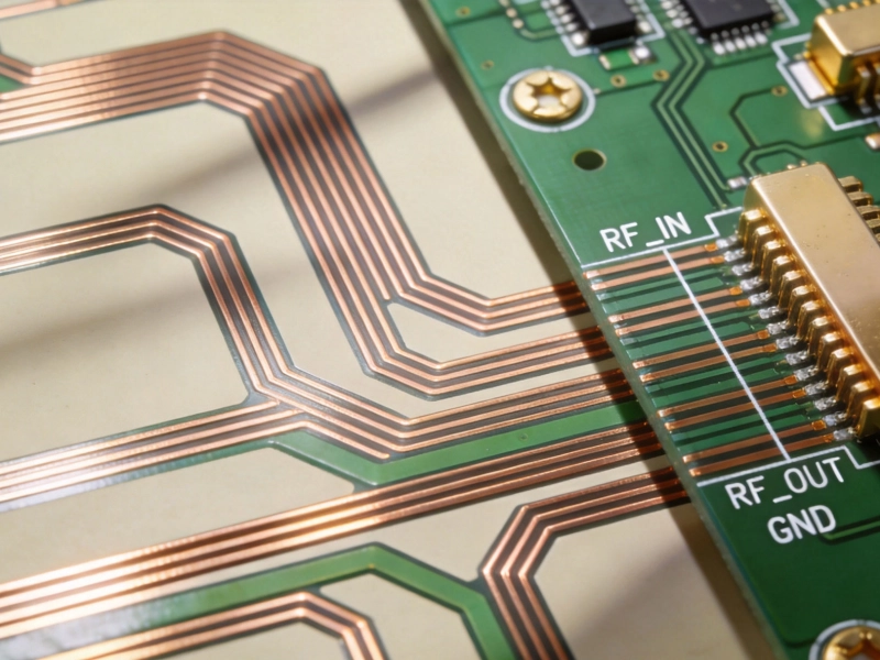
Coupled line structures— used in directional couplers, filters, and certain sensors— require tight control over trace spacing. The manufacturing capability for trace spacing varies significantly between Chinese factories. Standard PCB fabrication typically guarantees trace spacing tolerance of ±0.5 mils to ±1 mil. For coupled line couplers requiring specific coupling factors, this tolerance may be inadequate. Specify your spacing tolerance requirements explicitly and validate your manufacturer's capability before finalizing your design.
Blind and buried vias enable sophisticated RF designs but increase manufacturing complexity and cost dramatically. Not all Chinese prototype houses offer these technologies; those that do often have minimum order requirements or extended lead times. Always explore whether your RF design can achieve its goals with through vias before committing to blind/buried via structures. The cost and schedule implications are substantial.
Schematic-driven design works for many circuits, but high frequency structures often behave in ways that circuit simulation cannot predict. Electromagnetic simulation— using tools like HFSS, CST, or open-source alternatives— provides insight that circuit simulators miss. Structures operating at microwave frequencies fundamentally require EM analysis; treating them with lumped-element circuit models invites failure.
Even simple structures like bends, T-junctions, and vias benefit from EM simulation. The discontinuities these structures introduce can be quantified and compensated in your layout. Without simulation, you won't know whether a 90-degree bend introduces 0.1 dB of loss or 2 dB— a difference that matters enormously in receiver front ends where every decibel counts.
EM simulation requires accurate material models and boundary conditions. Your substrate library may contain default values that don't match your actual laminate. Always validate your simulation setup with measurements on known structures before trusting simulation results for your production design. The correlation between simulation and measurement determines how aggressively you can optimize your design.
Working with Chinese prototype houses requires explicit communication that domestic suppliers may not need. Cultural and linguistic differences can introduce ambiguity where none should exist. Technical terms translate imprecisely; assumptions go unstated. The result: prototypes that don't match specifications because specifications weren't communicated clearly.
Before placing your prototype order, hold a design review call or video conference with your manufacturer's engineering team. Walk through your critical parameters— impedance tolerances, material selections, critical dimensions. Ask them to repeat back their understanding of your requirements. This simple verification step catches miscommunications before they become expensive prototype failures.
Documentation quality matters. Provide your Chinese manufacturer with complete documentation packages including Gerber files, drill files, stack-up drawings, and impedance specifications. Don't assume they'll know what "standard high frequency practice" means— document exactly what you need. When you specify requirements clearly, you get results that meet requirements. When you leave room for interpretation, you get whatever interpretation the factory finds most convenient.
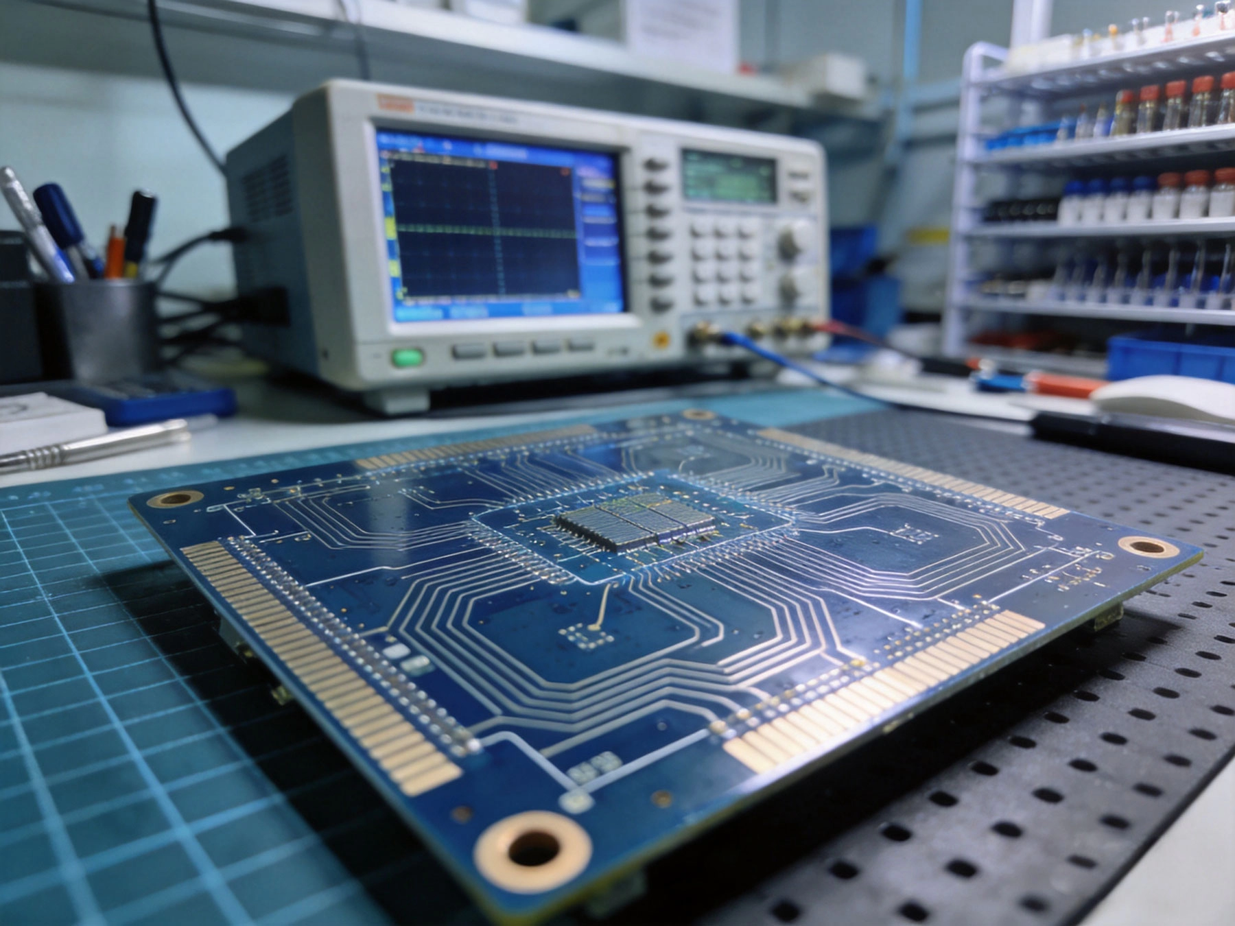
Prototype testing in high frequency designs must be thorough and systematic. A vector network analyzer becomes essential for characterization; a simple continuity tester tells you nothing about impedance matching or insertion loss. Many engineers receive prototypes that pass basic continuity tests, ship them for system integration, and discover RF problems that should have been caught during prototype verification.
Test structures on your prototype boards provide valuable data beyond your actual circuit. Include thru-reflect-line calibration structures, impedance test lines, and blank areas with your stack-up. These test structures allow you to validate material properties, manufacturing tolerances, and measurement techniques. When your circuits perform as expected, these structures confirm why. When circuits fail, test structures help diagnose whether the problem is design, manufacturing, or measurement error.
Environmental testing matters for high frequency prototypes. Dielectric properties change with temperature; thermal expansion affects dimensional tolerances. If your application will see temperature extremes, test prototypes across your operating temperature range. Chinese prototype houses can expedite thermal testing if you request it before manufacturing. Finding thermal issues during prototype testing costs a fraction of discovering them during field deployment.
High frequency PCB design inherently requires multiple prototype iterations. Expecting first-prototype success is unrealistic for complex RF designs. Budget and schedule for at least two or three prototype spins before reaching production-ready designs. Engineers who rush the process often spend more time and money fixing rushed decisions than they save by cutting prototype cycles short.
Each iteration should address specific questions. Your first prototype might validate coarse design decisions— layer stack, major component placement, connector types. Your second prototype refines details— trace geometries, component values, tuning elements. By the third iteration, you're optimizing performance and validating manufacturing consistency. Skipping early iterations to "save time" typically extends total project duration when problems surface late.
Document lessons learned from each prototype iteration. High frequency design knowledge accumulates through experience, but only if you capture that experience systematically. After each prototype test, record what worked, what failed, and what you'll do differently next time. This practice builds organizational knowledge that accelerates future projects and prevents repeating the same mistakes.
High frequency Pcb Prototyping presents challenges that standard digital design doesn't encounter. Success requires attention to fundamentals— material selection, impedance control, via management— while avoiding the shortcuts that work in lower-frequency designs. Working with Chinese manufacturers adds the requirement of clear communication and appropriate manufacturing partner selection.
The pitfalls described here have ended countless promising projects and frustrated talented engineers. By understanding where others have failed, you position yourself to avoid those same traps. Plan meticulously, specify precisely, and verify thoroughly. These practices separate successful high frequency designs from expensive prototype failures.
Your relationship with your Chinese prototype house shapes your outcomes as much as your schematic and layout. Choose manufacturing partners with demonstrated high frequency capability, communicate requirements explicitly, and verify understanding before production begins. With the right approach, the challenges of high frequency Pcb Prototyping become manageable— and the resulting designs perform reliably in the demanding environments where microwave and RF technology operates.
The Benefits of Rapid High Frequency PCB PrototypingMay/29/2026
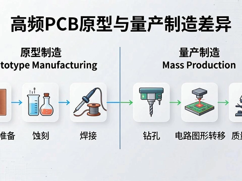
High Frequency PCB Prototype vs. Mass Production: Key Differences in FabricationJune/05/2026
Essential High Frequency PCB Knowledge for Hardware Engineers and DesignersMay/29/2026
Why Certifications Matter: IATF16949 and ISO Standards for Your High Frequency PCB ManufacturerJune/17/2026
Pushing the Limits: Our Latest High Frequency PCB Capabilities for 6G ResearchJune/11/2026
Handling Sensitive ComponentsMay/29/2026

Our Latest High Frequency PCB Capabilities for 6G ResearchMay/29/2026
Advanced High Frequency PCB Fabrication Techniques for Low Loss PerformanceMay/29/2026