Open Nav
High Frequency Pcb prototypes live or die by your Gerber files. Unlike standard digital boards where minor variations don't break anything, microwave and RF designs operating above 1 GHz are unforgiving. A trace that's 0.1mm off in width, a via that's slightly oversized, or a ground plane with an unexpected slot can turn your carefully simulated design into an expensive dead-end.
Getting Gerber files right for high frequency applications isn't about using different software—it's about understanding what the fabrication house needs to hit your impedance targets and maintain Signal Integrity at frequency. This guide walks you through the specific requirements that matter for RF and microwave prototype work.

At low frequencies, a PCB is just a collection of wires. At 5 GHz, 10 GHz, or 77 GHz Automotive Radar frequencies, your board becomes a transmission line network where every geometry decision affects performance. The Dielectric Constant of your material, the precise width of your traces, the spacing between signal and return paths—all of these become critical parameters.
When you submit Gerber files for a high frequency prototype, you're not just asking the factory to make boards. You're asking them to hit specific impedance values, typically 50 ohms for standard RF interconnects. If your files don't communicate exactly what you need, you get boards that look correct but perform wrong. That $500 prototype becomes a debugging nightmare when your insertion loss is 3 dB higher than expected.
Most PCB fabrication houses have Design for Manufacturability checks optimized for digital designs. These checks ensure traces aren't too fine, pads aren't too close, holes are within tolerance. But they don't catch the things that matter for RF: impedance discontinuities, via stub resonances, or insufficient ground reference spacing.
You need to be the expert on your design. This means understanding enough about high frequency behavior to specify your requirements clearly, and to catch errors in your own Gerber output before submission.
Before generating any Gerber files, nail down your layer stack. For high frequency work, this isn't a rough estimate—it's a precise specification that goes to the fabricator.
Standard FR-4 has a Dielectric Constant (Dk) that varies with frequency and isn't well-controlled, typically ranging from 4.2 to 4.6 with significant tolerance. For prototypes above 5 GHz, you want a high frequency laminate with tighter Dk tolerance. Common choices include:
Your Gerber files should reference a specific material, and you should discuss this with your prototype shop before submission. They need to know what they're working with to calibrate their processes.
For 50-ohm Controlled Impedance traces, you need to specify not just the trace width, but also the dielectric thickness below and above the trace, the copper weight, and the dielectric constant. This stackup information should accompany your Gerber files as a separate document.
Here's the critical part: include both your calculated trace width AND the target impedance in your documentation. If the fabricator's process ends up with slightly different dielectric thickness than your calculation assumed, they can adjust trace width to hit the impedance target rather than blindly manufacturing to your specified width.
High frequency prototypes typically need more layers specified than standard boards, and some layers that are optional for digital work become essential.
For a typical high frequency board, include these layers:
Ground planes are more critical in RF designs than in digital work. Your Gerber files need continuous, unbroken ground reference beneath all RF traces. Small gaps or slots in ground planes create impedance discontinuities that radiate and cause interference.
When reviewing your Gerber output, look specifically for thermal relief patterns on ground planes. Standard thermal relief (the spokes connecting surface pads to internal planes) creates inductance at high frequencies. For RF prototype work, specify solid ground connections where it matters, and make this clear in your fab notes.
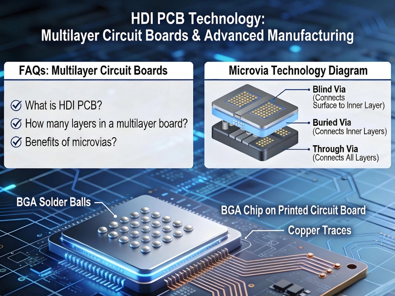
Vias are one of the biggest challenges in High Frequency Pcb design. Every via creates an impedance discontinuity, and the via stub can act as a resonant stub at certain frequencies.
When generating your drill files, specify vias with dimensions appropriate for your frequency range:
For critical RF paths, back-drilling or blind/buried vias eliminate the stub problem entirely, but these increase cost significantly. For most prototype work, proper via sizing is sufficient—keep vias short and specify adequate anti-pad clearance.
Place ground vias immediately adjacent to signal vias on high frequency nets. This technique, called "via stitching," provides a return path that minimizes loop area and reduces inductance. In your Gerber output, add these stitching vias manually if your EDA tool doesn't place them automatically.
Specify via spacing in your fab notes: typically one ground via within 2-3 mm of the signal via for frequencies up to 20 GHz. The closer, the better for Signal Integrity.
High frequency prototypes require tighter trace width tolerance than standard boards. A 10% variation in trace width on a 50-ohm line causes measurable impedance variation.
When submitting Gerber files, include tolerance specifications on critical dimensions:
The fabricator needs to know which dimensions are critical. A connector pad that's 0.3mm vs 0.35mm isn't a problem, but a 50-ohm trace at 0.35mm vs 0.30mm matters enormously.
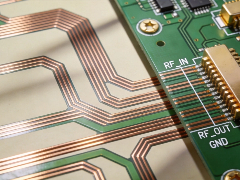
If your design includes coupled transmission lines (for baluns, directional couplers, or differential pairs), specify the coupled section dimensions with particular care. These structures are sensitive to both trace width and spacing variations, and the two interact to determine the characteristic impedance and coupling factor.
Include a cross-section diagram in your fab package showing the intended stackup geometry for all critical coupled sections. This eliminates ambiguity about what you're trying to achieve.
Gerber files alone are insufficient for high frequency prototype success. You need supporting documentation that tells the fabrication house what you actually need.
Create a fabrication drawing that includes:
This documentation doesn't need to be fancy, but it needs to be complete. The goal is answering every question a process engineer might have without requiring them to ask.
Some EDA tools allow you to embed net attributes in the Gerber output or provide a separate net attribute file. If your tool supports this, specify impedance-controlled nets and their target values. Even if the fabricator doesn't use this information directly, it forces you to document your requirements clearly.
Having seen high frequency prototypes fail for predictable reasons, here are the mistakes to avoid:
Most EDA tools use simplified models for impedance calculation that don't account for the full geometry including solder mask effects, manufacturing variations, or dielectric anisotropy. Use a dedicated transmission line calculator (like Polar Instruments' SI9000 or similar) for critical impedance lines, and cross-check against your EDA tool's result. When they differ, investigate why.
Always view your exported Gerber files in a neutral CAM viewer (like Gerbv, ViewMate, or your fabricator's online viewer) before submission. Check that all layers are present, the board outline is correct, and there are no unexpected features. What you see in your EDA tool isn't always what gets exported.
Silkscreen ink adds a thin dielectric layer over your traces. For very high frequency work (above 20 GHz), this affects effective dielectric constant and impedance. If you're working at these frequencies, specify silkscreen removal over critical RF traces, or specify a thinner silkscreen application.
When routing with angled corners, your EDA tool may break long traces into multiple segments. While this is fine electrically, it can create artifacts in manufacturing. Specify mitered 45-degree corners rather than 90-degree corners, and minimize the number of segments on critical RF paths.
The relationship between designer and fabricator matters more for high frequency prototypes than almost any other PCB type. Here's how to make it productive:
Before sending your Gerber files, send your documentation package to the fabricator's engineering team. Ask them to review your stackup and impedance specifications. Their process capabilities may require adjustments—better to find out before manufacturing than after.
Many high frequency prototype shops offer impedance testing on sample coupons. Budget for this. Spending $100-200 on impedance verification saves debugging time on your $2000 prototype assembly.
If you're ordering multiple designs in a panel, be aware that routing between boards can affect ground plane integrity. Specify additional copper tie points between panel rails and board grounds if ground continuity matters for your design. This isn't necessary for every design, but for sensitive RF boards, it's worth discussing.
Establish impedance test criteria with your fabricator before manufacturing. What impedance tolerance is acceptable? 5%? 10%? This needs to be agreed upon upfront, because impedance testing isn't binary—it produces a range of values, and you need to define pass/fail criteria.
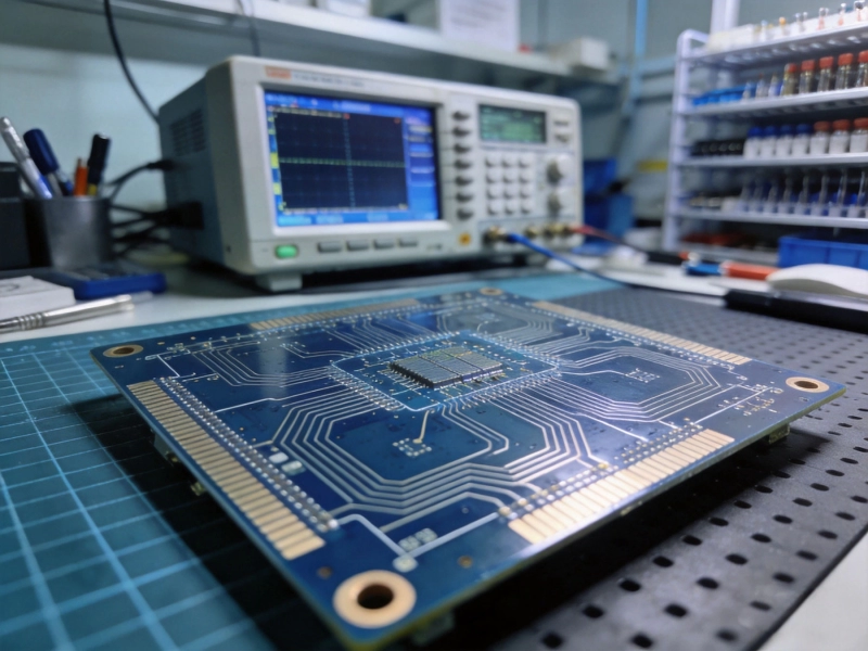
Even with perfect Gerber files and careful fabrication, prototype testing is essential. High frequency boards often exhibit behavior that simulations don't predict perfectly.
Before electrical testing, verify physical dimensions. Use a digital micrometer to measure dielectric thickness at several points. Inspect trace widths under a microscope if possible. A 5% deviation in dielectric thickness from one area of the board to another isn't unusual and can cause impedance variations across your design.
TDR testing reveals impedance discontinuities along a transmission line. If you have access to a TDR or a network analyzer with TDR capability, probe your critical RF nets. Unexpected impedance bumps indicate problems—sometimes in the board, sometimes in your test setup. Knowing how to interpret TDR traces is a valuable skill for high frequency prototype debugging.
Compare measured insertion loss against your simulations. Significant differences (more than 1-2 dB at your operating frequency) indicate issues: wrong material properties, surface roughness losses higher than expected, or manufacturing variations. Document these differences—they inform your next design iteration.
Preparing Gerber files for high frequency PCB prototypes requires more attention to detail than standard PCB work, but the requirements are straightforward once you understand them:
High Frequency Pcb Prototyping is demanding, but the gap between simulation and reality is narrower than many designers fear. With careful Gerber preparation, clear communication with your fabrication partner, and thoughtful testing, you can close that loop and get prototypes that perform as expected. The fundamentals aren't complicated—but the discipline to follow them matters.
Above 1 GHz, start considering Controlled Impedance and RF-specific stackup. Above 5 GHz, every geometry decision matters and you should apply all the practices in this guide. Below 1 GHz, standard fabrication tolerances are usually acceptable, though controlled impedance can still matter for certain clock and high-speed digital signals.
You can, but with clear understanding of the limitations. FR-4's Dk varies with frequency (called dispersion), varies between batches, and has wider tolerance than high-frequency laminates. For prototypes below 10 GHz where performance targets aren't aggressive, FR-4 can work. For anything demanding, specify a purpose-made high frequency material.
High frequency materials cost 3-10x more than FR-4 per panel. Controlled impedance processing adds 20-40% to fabrication cost. Tight tolerances add more. Via-in-pad or back-drilling adds significant cost. Budget accordingly—high frequency prototypes are expensive, which is why getting the Gerber files right matters so much. A respin costs as much as the first run.
ENIG (electroless nickel gold) is most common. The nickel layer provides a reliable surface that solders well and resists oxidation. Immersion silver has slightly better electrical performance at very high frequencies but tarnishes over time. For prototypes that will be assembled and tested relatively quickly, either works. For anything stored before assembly, ENIG's shelf stability is an advantage.
±10% is achievable at most prototype shops without special processes. ±5% requires a shop with good process control and may cost extra. ±2% requires very tight material control and is premium territory. Most RF designs function acceptably at ±7-10%, but if you're designing a 77 GHz Automotive Radar, tighter tolerances matter more than for a 5 GHz WiFi frontend.
The Benefits of Rapid High Frequency PCB PrototypingMay/29/2026
Common Pitfalls to Avoid During Your High Frequency PCB Prototype PhaseJune/18/2026
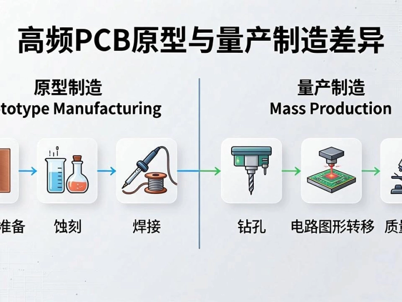
High Frequency PCB Prototype vs. Mass Production: Key Differences in FabricationJune/05/2026
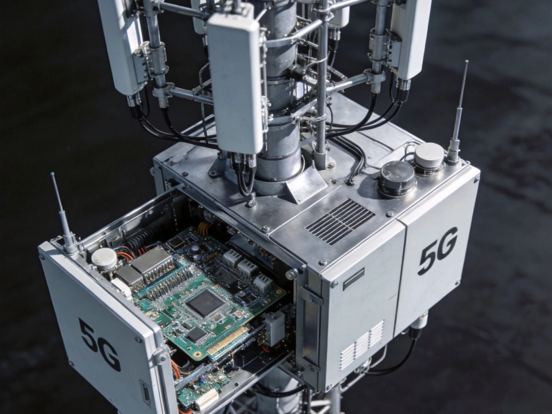
Top High Frequency PCB Applications in the 5G and Telecommunications IndustryMay/29/2026
The Challenges of High Frequency PCB Assembly: Handling Sensitive ComponentsMay/29/2026
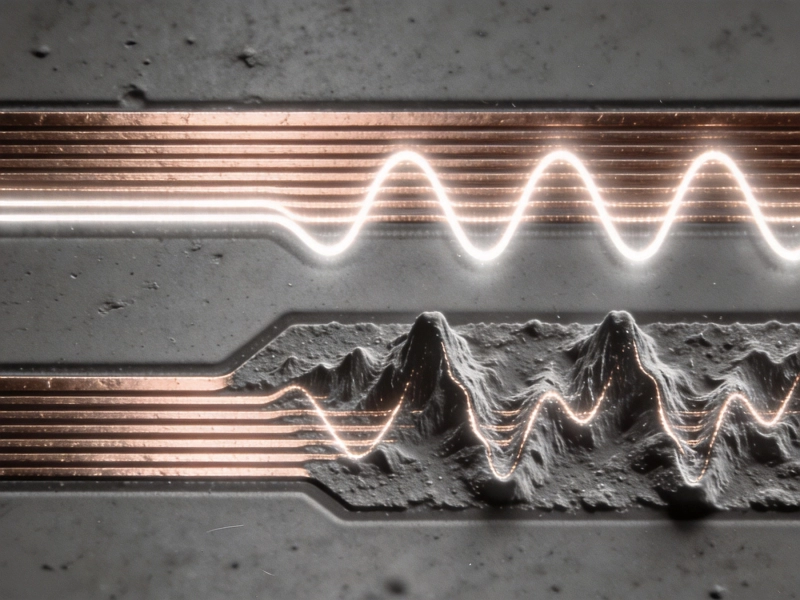
The Impact of Surface Roughness on High Frequency PCB Fabrication QualityJune/27/2026

Essential High Frequency PCB Knowledge for Hardware Engineers and DesignersJune/15/2026
Handling Sensitive ComponentsMay/29/2026