Open Nav
In the race to bring 5G networks, advanced driver assistance systems, and next-generation wireless products to market, speed is everything. Every week of delay in research and development translates directly into lost competitive advantage, extended time-to-market, and foregone revenue. Yet the unique challenges of High Frequency Pcb design — with their demanding material requirements, tight impedance tolerances, and specialized manufacturing processes — have traditionally made rapid prototyping difficult to achieve. This guide explores how modern rapid High Frequency Pcb prototyping services are changing the equation for engineering teams, enabling faster iteration cycles and shorter development timelines for RF and microwave applications.
Standard Pcb Prototyping has become remarkably fast. Online fabrication services can produce simple multilayer boards in 24-48 hours, and even complex boards typically ship within 5-7 working days. But high frequency PCBs operate under different constraints that challenge conventional quick-turn approaches.
High Frequency Pcb Materials like Rogers RT/duroid, Rogers RO4000 series, Taconic RF laminates, and hydrocarbon ceramic composites are specialty items that most standard PCB shops do not stock. Ordering these materials from distributors adds lead time before manufacturing can even begin. A manufacturer with deep inventory of common RF materials can begin production immediately, while one that must source materials externally adds days or weeks to the timeline.
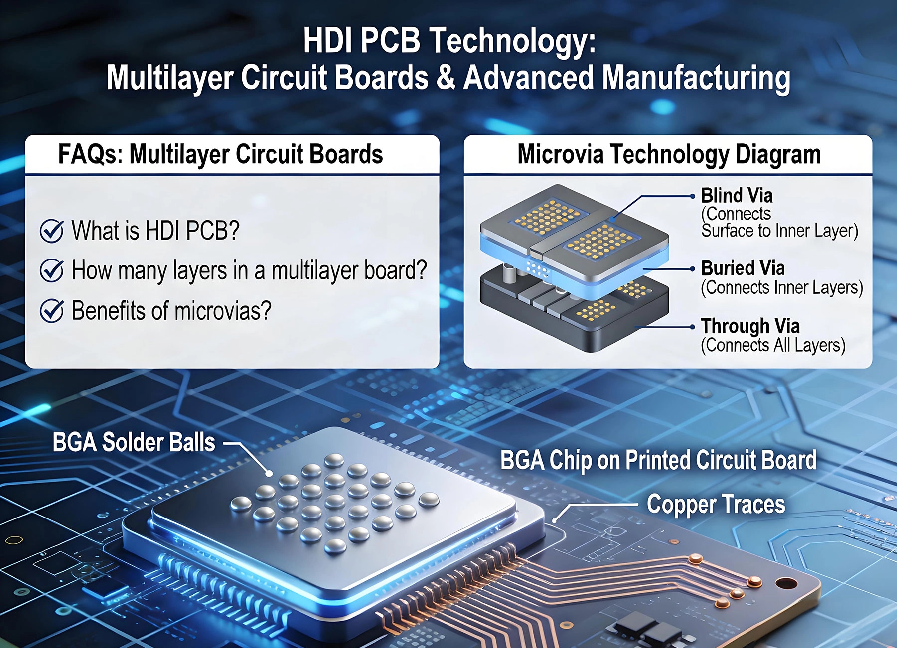
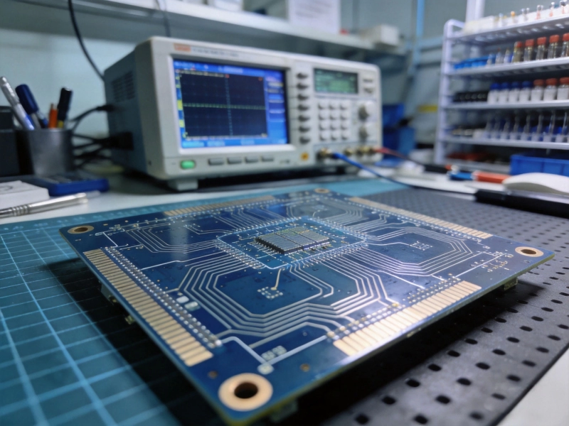
RF Pcb Manufacturing involves processes that standard PCB shops may not have optimized. Laser drilling for blind vias in RF laminates, Controlled Impedance testing with TDR equipment, low-roughness copper processing for minimum insertion loss — these capabilities require specialized equipment and process expertise that not all manufacturers possess. The learning curve for manufacturing RF boards correctly at the first attempt is steep, and inexperienced shops may require multiple iterations to produce acceptable boards.
Unlike standard digital PCBs where visual inspection suffices, high frequency boards require electrical testing that takes time. Time domain reflectometry (TDR) testing for impedance verification, insertion loss measurements, and documentation of test results all add to the production cycle. Cutting corners on testing to save time risks shipping boards that do not meet specifications — which ultimately wastes more time than proper testing saves.
Rapid high frequency Pcb Prototyping refers to accelerated manufacturing services specifically designed for RF and microwave circuit boards, with lead times significantly shorter than standard production. These services combine deep material inventory, optimized Rf Manufacturing processes, streamlined quality verification, and dedicated capacity to deliver functional prototype boards in days rather than weeks.
The most immediate benefit of rapid RF prototyping is faster design iteration. Engineering is fundamentally iterative — you design, you build, you test, you learn, and you redesign. When each iteration takes three weeks, you might achieve three or four design cycles in a product development program. When each iteration takes one week, you might achieve eight to ten cycles in the same timeframe.
For high frequency PCB development, this iteration speed is particularly valuable because RF performance is highly sensitive to subtle design details. The exact pad geometry that affects impedance match, the via fence spacing that influences isolation, the trace routing that determines coupling — these factors often require empirical adjustment based on measured performance. Rapid prototyping enables this empirical optimization to happen at the speed the design process demands.
Design errors discovered late in development are exponentially more expensive to fix than errors found early. A routing error that requires layout changes costs a few hours of engineering time if caught during initial design. The same error, discovered after the board is fabricated, costs engineering time plus board fabrication cost plus schedule delay. Discover it after the board is assembled, and you add component cost and assembly labor to the tally.
Rapid prototyping enables more frequent check-points where design issues are surfaced before they become expensive problems. The cost premium for quick-turn prototyping is almost always less than the cost of a single development program delay.
In fast-moving markets like 5G, Automotive Radar, and consumer wireless, being first to market provides sustained competitive advantage. A product that ships six months before a competitor captures market share, establishes brand recognition, and forces competitors to catch up from behind. A product that ships six months late may find the market already captured by established competitors.
Rapid RF PCB prototyping directly supports faster time-to-market by compressing the prototype and validation phases of product development. Engineering teams can complete more design iterations, achieve higher design confidence, and reach production release faster than competitors constrained by longer prototype lead times.
When prototype boards take three weeks to arrive, there is strong pressure to minimize the number of prototypes — to make each board count as much as possible. This pressure can lead to inadequate testing, with the result that marginal designs proceed to production without full validation.
When prototype boards arrive in one week, it becomes practical to build multiple boards for different purposes: one for electrical performance validation, one for thermal testing, one for mechanical fit checking. This comprehensive verification approach reduces the risk of discovering problems in production or, worse, in the field.
Engineers working on projects with long prototype cycles develop coping behaviors that reduce productivity. They batch design changes to minimize prototype orders, deferring design decisions until they can be included in the next build. They spend time on simulation and analysis that would be unnecessary if they could simply build and measure. They multitask across projects while waiting for boards, fragmenting their focus.
Short prototype cycles eliminate these productivity drains. Engineers make decisions when they are ready, not when the prototype schedule forces them. They spend time building and testing real hardware rather than simulating what they would measure if they could build. Their focus is sharp because they are working on one project rather than waiting on several.
Engineering teams that use rapid prototyping services develop closer relationships with their manufacturing partners. The faster cadence of interaction builds mutual understanding that benefits both parties. Engineers learn what designs are manufacturable and what designs cause problems. Manufacturers learn what engineers need and can anticipate problems before they occur.
These relationships become more valuable as products move from Prototype To Production. A manufacturer that knows your design philosophy, your quality requirements, and your schedule pressures is a better production partner than one that is starting from scratch.
The early stages of RF PCB development benefit most from rapid prototyping because design concepts are fluid and likely to change. Rapid prototype boards allow exploration of multiple architectural options, enabling engineering teams to make informed decisions about which approach to pursue based on measured performance rather than simulation alone.
Before committing a design to production, verification prototypes confirm that the final design meets all performance requirements. Rapid prototyping ensures that verification can proceed on schedule, avoiding the common problem of verification being compressed because prototype boards arrived late.
Design changes discovered during verification testing require new prototype boards. Rather than treating these changes as schedule risks, engineering teams with access to rapid prototyping can incorporate changes quickly, keeping the program on schedule.
For products with low production volumes, rapid prototyping services can sometimes serve as the production source, avoiding the tooling costs and minimum order quantities of standard production. This approach is particularly valuable for prototype quantities of custom RF assemblies.
When production boards are unavailable due to supply chain disruptions or design changes, rapid prototyping services can produce replacement boards quickly, keeping customer systems operational while production recovers.
Rapid prototyping services operate most efficiently when design documentation is complete and unambiguous. Provide:
Incomplete documentation causes delays as the manufacturer seeks clarification, eliminating much of the time savings that rapid prototyping provides.
Share your design with the rapid prototyping service early, before placing the order. Many manufacturers offer informal Dfm feedback that identifies potential manufacturing issues before they cause delays. This feedback is most valuable early in the design cycle, when changes are least expensive to implement.
Some PCB features cannot be manufactured faster regardless of priority. Laser drilling and plating processes take the time they take. Sequential lamination cycles cannot be skipped. Tdr Testing requires equipment time regardless of how much you are willing to pay. Understanding what can and cannot be expedited prevents unrealistic expectations and disappointment.
The value of rapid prototyping compounds when you commit to multiple iterations from the beginning. Plan for at least two or three prototype builds, with each build incorporating lessons from the previous one. This commitment justifies the cost premium for rapid service and maximizes the learning that each build enables.
Rapid prototyping does not replace simulation — it complements it. Investment in accurate electromagnetic simulation before the first prototype reduces the number of iterations required and makes each iteration more productive. Use simulation to narrow the design space, then use rapid prototyping to validate and refine the design.
Rapid prototyping accelerates design iteration, but it does not replace the need for sound engineering. Teams that rely entirely on build-and-fix without adequate simulation and analysis often require more iterations, not fewer, because they are chasing issues that could have been predicted.
Receiving a prototype board quickly is valueless if there is not adequate time to test it thoroughly before the next prototype is needed. Build testing time into the schedule, and resist the temptation to compress testing to rush the next build.
Each prototype iteration should address a specific set of design questions. Frequent requirement changes between iterations waste prototype builds and slow learning. Establish stable design requirements before ordering prototypes, and change them only for compelling reasons.
Each prototype iteration generates valuable information about what works and what does not. Engineering teams that do not document these lessons lose the benefit of their prototyping investment. Create formal lessons-learned records for each prototype build, and review them before starting the next iteration.
Rapid prototyping services typically cost 50-200% more than standard production lead times for equivalent boards. This premium reflects:
The rapid prototyping premium is justified when:
Standard lead times are appropriate when:
Rapid high frequency PCB prototyping has become an essential capability for engineering teams developing RF and microwave products. The benefits extend beyond simple speed — rapid prototyping enables faster design iteration, reduces development cost through earlier problem detection, supports competitive time-to-market, enables comprehensive verification, improves engineering productivity, and builds stronger supplier relationships.
When selecting a rapid prototyping partner, look for manufacturers with deep RF material inventory, proven high frequency manufacturing capabilities, reliable lead time commitments, and responsive engineering support. The right partner transforms your prototype program from a source of schedule risk into a competitive advantage that accelerates your path to market.
In high frequency electronics development, the team that can learn fastest wins. Rapid prototyping is how you accelerate that learning.
Common Pitfalls to Avoid During Your High Frequency PCB Prototype PhaseJune/18/2026
Why Impedance Control is Critical Even in High Frequency PCB PrototypesJuly/14/2026

How to Prepare Gerber Files for a Successful High Frequency PCB PrototypeJuly/02/2026
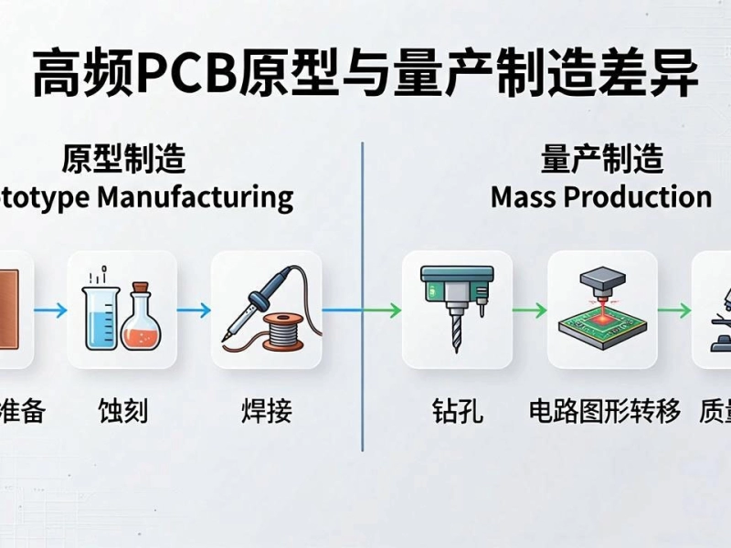
High Frequency PCB Prototype vs. Mass Production: Key Differences in FabricationJune/05/2026
Demystifying Impedance Control: Core High Frequency PCB KnowledgeJuly/09/2026
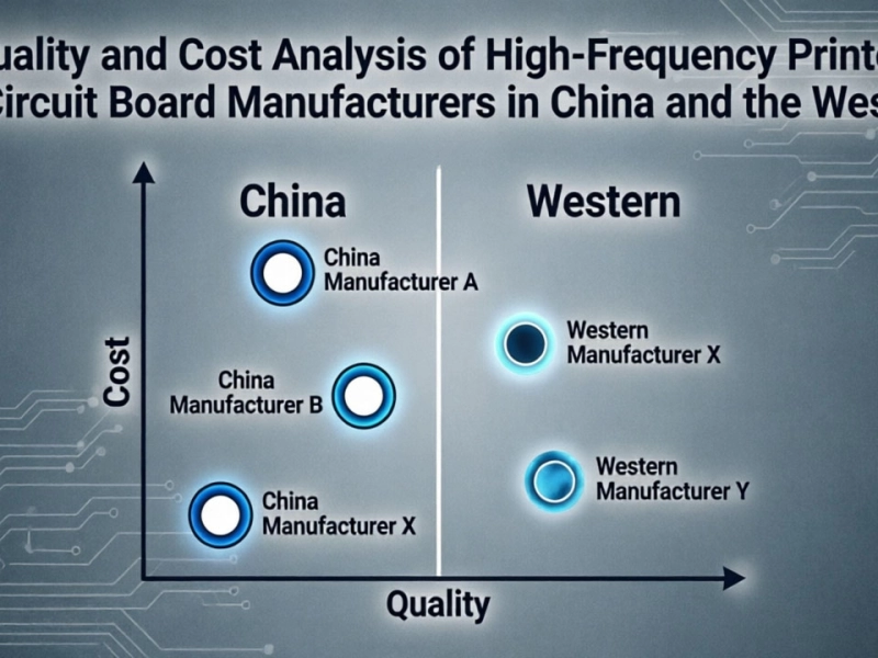
Quality and Cost Analysis of High-Frequency Printed Circuit Board Manufacturers in China and the WestJune/04/2026
Understanding High Frequency PCB Capabilities: Line Width, Spacing, and Layer CountJune/28/2026
Laser Drilling and Microvias in Modern High Frequency PCB FabricationJuly/07/2026