Open Nav
High frequency printed circuit boards operate in an entirely different engineering universe compared to standard digital boards. While a typical microcontroller PCB worries about getting signals from point A to point B without opens or shorts, a High Frequency Pcb must ensure that the signals arrive at point B with the right impedance, at the right time, with minimal loss and no unintended radiation. That is a fundamentally harder problem, and it starts with understanding — down to the micron — what the manufacturing process can and cannot reliably produce.
When design engineers approach our team about high frequency or RF (Radio Frequency) PCB fabrication, the most common questions revolve around three tightly interrelated topics: trace line width tolerances, trace spacing capabilities, and the layer count required to route complex signals cleanly. These are not independent variables. Change one, and it reshapes the engineering landscape for the other two.
This article walks through each of these capability areas in practical terms — not just what the spec sheets say, but what it actually means for your design, your yield, and your end product's RF performance.
The term "high frequency" in PCB design typically kicks in above 100 MHz, and becomes critical above 1 GHz. At these frequencies, the wavelength of the signal approaches the physical dimensions of the traces themselves. When that happens, the PCB trace stops behaving like a simple wire and starts behaving like a transmission line.
At low frequencies, a trace is just a conductor carrying current from one component to another. At high frequencies, every physical characteristic of that trace — its width, its height above the reference plane, the Dielectric Constant of the material surrounding it, and its proximity to adjacent traces — becomes part of the electrical performance equation. That is why High Frequency Pcb Capabilities matter. The manufacturing precision required to hit those electrical targets is orders of magnitude higher than what standard FR-4 production demands.
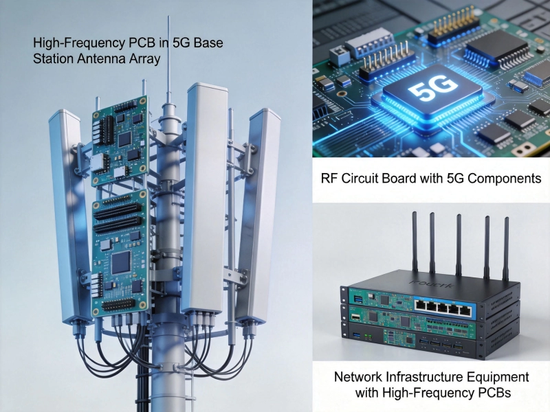
Common applications that require High Frequency Pcb design include:
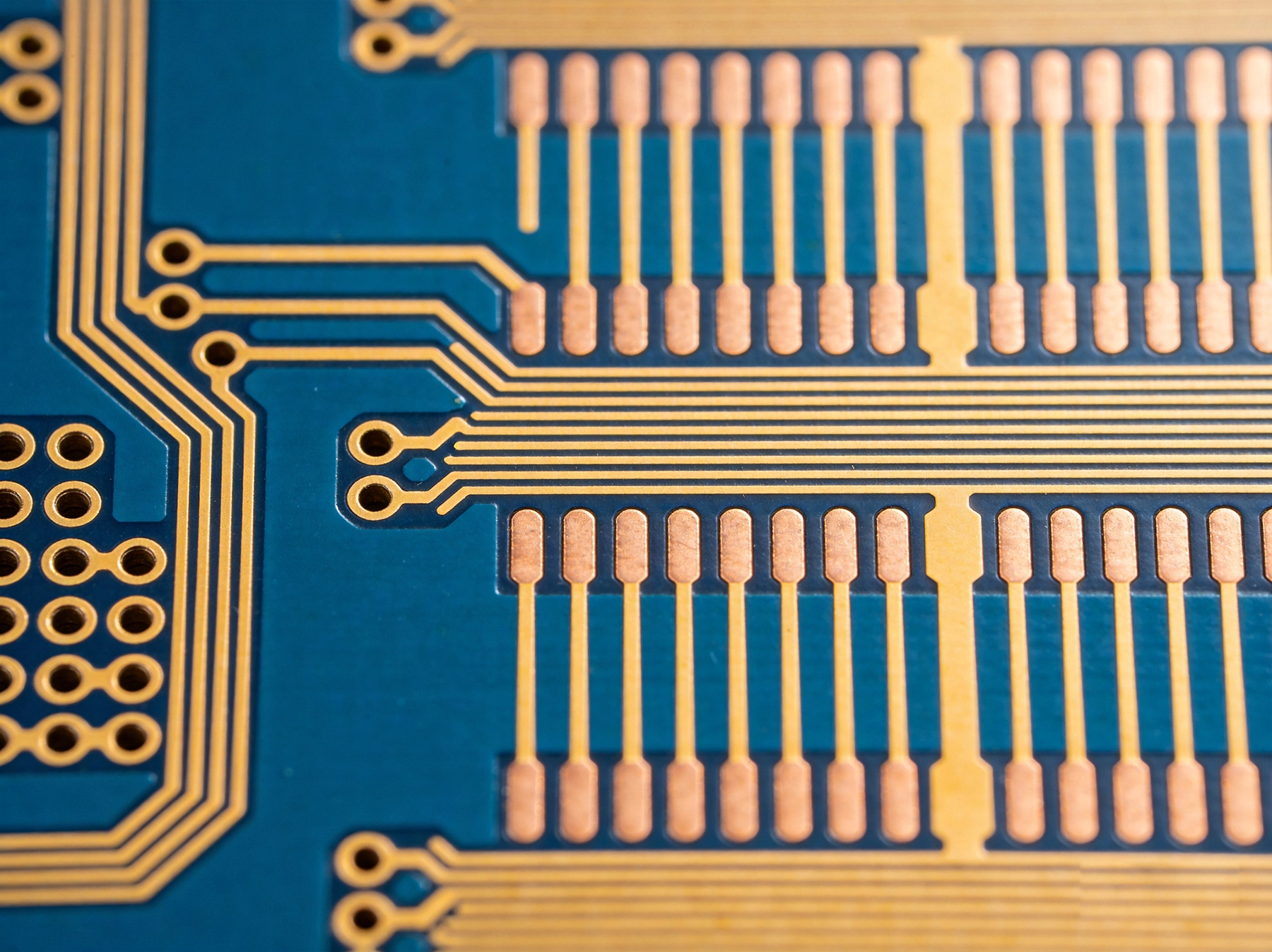
In a standard digital PCB, a trace that is 10% wider or narrower than nominal is unlikely to cause any noticeable problem. At 10 MHz, the electrical impact of that variation is negligible. At 10 GHz — inside a 5G millimeter-wave module or an Automotive Radar sensor — that same 10% width variation can shift the characteristic impedance of a 50-ohm trace by 3 to 5 ohms. For a 50-ohm system, that is a significant impedance mismatch that sends reflected signals back toward the source, degrades Signal Integrity, and generates unwanted electromagnetic radiation.
High frequency PCB manufacturers must therefore control trace width to tolerances that would be considered unnecessary overengineering for standard boards. In practice, this means tighter process controls, more frequent calibration of imaging and etching equipment, and statistical process monitoring throughout the production run.
The line width that a fabricator can reliably achieve depends on the substrate material and the overall complexity of the board. Here is a practical reference based on what most specialized high frequency PCB manufacturers in China can deliver:
It is important to distinguish between the minimum achievable trace width on a given material and the width that can be produced with tight impedance tolerance. A fabricator might be able to etch a 2-mil trace on Rogers material, but maintaining ±5% impedance tolerance on a 2-mil 50-ohm line is a much harder engineering challenge than doing the same on a 6-mil trace. When evaluating a manufacturer for high frequency work, always ask about their impedance tolerance capability — not just their minimum trace width.
Controlled Impedance is the primary reason line width precision matters in high frequency designs. The characteristic impedance of a microstrip trace is determined by the interplay of trace width (W), trace thickness (T), dielectric height (H), and the Dielectric Constant (Dk) of the substrate material. For a 50-ohm microstrip line on a typical Rogers substrate:
The impedance equation for a microstrip trace is not linear — small percentage changes in width produce larger percentage changes in impedance at higher frequencies. This is why high frequency Pcb Manufacturing requires proactive impedance modeling before production, using the fabricator's specific material parameters and process data.
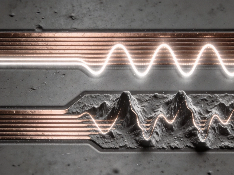
On a high frequency board, trace spacing is not just about preventing opens and shorts — it is about controlling electromagnetic coupling between adjacent traces. At microwave frequencies, two parallel traces act as unintended coupling elements. Energy from a high-speed signal trace can couple into a neighboring trace, creating crosstalk that corrupts sensitive receiver circuits or generates spurious emissions that violate regulatory standards like FCC Part 15 or CE EN 55032.
The coupling coefficient between two parallel traces depends on the spacing between them, the length over which they run parallel, and the frequency of the signal. For a given board stackup, the rule of thumb is that crosstalk drops roughly proportionally to the square of the spacing — double the gap, quarter the crosstalk. But increasing spacing costs routing density, which is always at a premium on complex RF boards.
What spacing can high frequency PCB manufacturers actually achieve? The answer varies by material and process, but here is a practical overview:
For RF and microwave designs, a highly effective strategy for controlling coupling is to route critical signals between continuous ground planes, with ground trace guarding where necessary. Ground-to-signal spacing of 2 to 3 times the dielectric height is typically sufficient to suppress unwanted coupling on signals up to 20 GHz. Above 20 GHz, even tighter coupling suppression is needed, and the board may require more complex multi-layer stackups with dedicated ground reference layers immediately adjacent to the signal layer.
In our work designing and fabricating boards for 77 GHz automotive radar applications, the signal-to-ground spacing on the critical transmit and receive paths is controlled to within ±0.2 mils — a level of precision that requires dedicated RF manufacturing facilities, not general-purpose PCB production lines.
The number of layers in a high frequency PCB is not simply a function of routing density — it is a fundamental RF engineering decision. Each additional layer in the stackup provides either more routing resource or more reference plane coverage, and in high frequency designs, the reference plane quality is often more important than routing capacity.
A well-designed high frequency stackup uses every layer strategically:
Here are the stackup configurations most commonly used in High Frequency Pcb Design, ranging from simple to complex:
Typical configuration: Signal (top) / Ground / Power / Signal (bottom)
Use case: Frequency range up to approximately 6 GHz. The single ground reference layer constrains impedance predictability but is adequate for many Wi-Fi, GPS, and ISM band applications. Cost-effective for lower complexity designs.
Typical configuration: RF Signal / Ground / Signal / Ground / Power / Signal
Use case: Frequency range from 6 GHz to 18 GHz. The dual ground reference layers allow much tighter Impedance Control and better isolation between RF and digital sections. Suitable for 5G sub-6GHz, point-to-point microwave backhaul, and most radar applications below 20 GHz.
Typical configuration: Multiple dedicated RF layers with ground-to-ground bonding between them, separated by low-contrast Dielectric Materials
Use case: Frequencies above 20 GHz, including 77 GHz automotive radar, 28 GHz and 39 GHz 5G Millimeter Wave, and E-band microwave. These stackups require sophisticated material selection (often mixing Rogers high-Dk and low-Dk materials), blind and buried vias, and very precise lamination control.
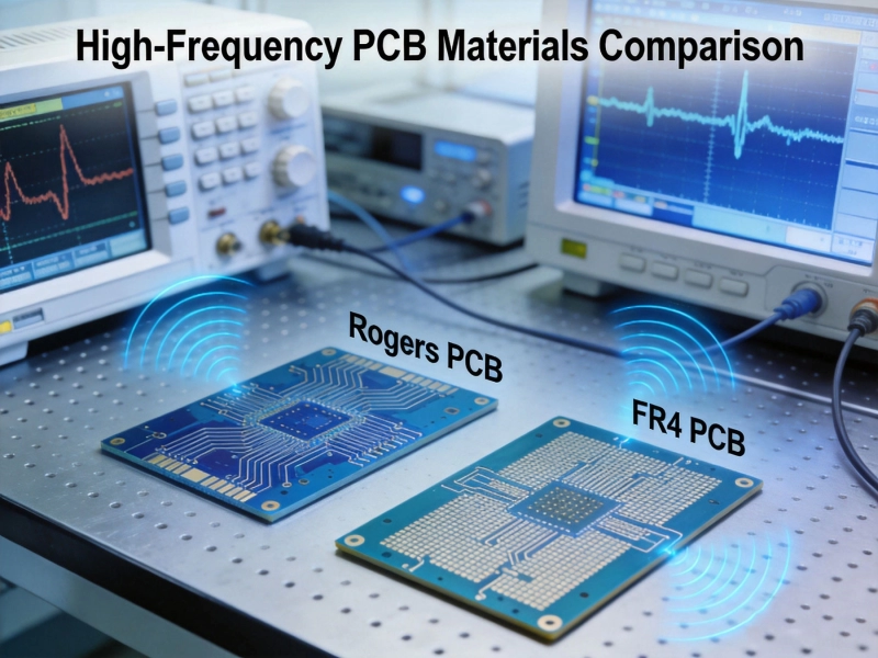
Layer count decisions are inseparable from dielectric thickness control. In a high frequency stackup, the thickness between the signal layer and its reference plane determines the impedance of the trace. Standard Pcb Materials like FR-4 have dielectric constant (Dk) that varies with frequency and temperature — a property called Dk dispersion. This makes FR-4 unsuitable for designs above approximately 10 GHz without extensive characterization and compensation.
High frequency substrates like Rogers RO4003C (Dk = 3.38) and RO4350B (Dk = 3.48) have much more stable Dk characteristics across frequency and temperature. The trade-off is cost — Rogers materials typically cost 5 to 15 times more per square foot than FR-4. When designing an 8-layer millimeter-wave board, the material selection and layer thickness optimization can involve weeks of electromagnetic simulation before a single board is fabricated.
Vias are necessary for connecting traces between layers, but at high frequencies they introduce discontinuities. The portion of the via barrel that extends below the signal layer — the "via stub" — acts as an unintended resonator. At frequencies where the stub length is approximately one-quarter wavelength, it presents a high impedance shunt that degrades signal quality.
For designs operating above 5 GHz, via stub management becomes critical. The standard solution is back-drilling — removing the stub portion of the via after plating by drilling it out to the reference layer. Advanced designs use blind vias (from the surface to an inner layer) or buried vias (connecting only inner layers) to eliminate stubs entirely.
When a trace transitions from the top layer to an inner layer through a via, the via geometry creates a capacitive discontinuity. The annular ring, anti-pad size, and pad diameter all affect the via capacitance. Designers working above 10 GHz typically run full-wave 3D electromagnetic simulations of via transitions to optimize the anti-pad geometry and ensure the via transition does not introduce unacceptable VSWR (Voltage Standing Wave Ratio) degradation.
At 77 GHz, even a well-designed via can introduce measurable loss. The pragmatic approach in millimeter-wave design is to minimize the number of layer transitions on critical RF paths and to use high-quality coaxial-like transitions (e.g., launch connectors) at the board edge rather than routing vias on the most critical signal paths.
High Frequency Pcb Capabilities are not just about the manufacturer's process — they are deeply tied to the substrate material properties. The three material parameters that matter most for high frequency performance are:
The dielectric constant of the substrate determines the propagation velocity and impedance of traces on that material. Rogers materials offer tight Dk tolerances of ±0.05 (compared to ±0.1 or looser for standard FR-4), which translates directly to more predictable impedance. Some manufacturers offer custom Dk profiling across a panel for advanced applications.
The loss tangent quantifies how much energy is dissipated as heat in the dielectric during each AC cycle. For high frequency signals, a lower loss tangent means less signal attenuation per unit length. Rogers Ro4350b has Df of 0.0037, while high-performance materials like RT/duroid 5880 achieves Df of 0.0009. At 28 GHz, this difference translates to roughly 30% less insertion loss per inch on RT/duroid versus RO4350B.
As the board temperature changes during operation (or during reflow assembly), the Dk of the material shifts. For applications in automotive radar or outdoor wireless infrastructure, this temperature stability is critical. Rogers materials have TCDk values of approximately +50 ppm/°C, meaning a 50°C temperature rise changes the Dk by only about 250 ppm — negligible for most applications.
The most successful high frequency PCB projects we have worked on share one common practice: early collaboration between the design team and the manufacturing engineering team at the fabricator. This is not a nice-to-have — it is a requirement for getting it right the first time.
A quality High Frequency Pcb Manufacturer will typically ask for:
Providing this information upfront allows the fabricator to run their own impedance modeling, select appropriate material lots (batches with consistent Dk), and build the production panels with the process controls needed to hit the targets.
Before releasing a high frequency design for fabrication, the following DRC checkpoints are essential:
High frequency PCB capabilities do not come free. The incremental cost of moving from standard FR-4 production to controlled-impedance RF fabrication is driven by several factors:
A well-balanced design balances performance requirements against cost reality. Not every 5 GHz design needs Rogers material — some designs can achieve adequate performance on high-quality modified FR-4 with careful impedance modeling. The key is making that assessment based on actual electrical requirements, not default habits or overspecification.
High frequency PCB capabilities — line width, spacing, and layer count — are the three pillars of Rf Pcb design that separate mission-critical communication systems from standard digital products. Line width precision determines whether you hit your impedance targets. Trace spacing controls coupling and prevents crosstalk. Layer count and stackup strategy define the RF environment your signals travel through.
None of these factors operates in isolation. The best high frequency designs treat manufacturing capability as a design input, not an afterthought. Engage early with a fabricator who specializes in RF and millimeter-wave boards. Share your impedance budgets, your frequency targets, and your thermal environment. Let their process data inform your stackup decisions, and you will arrive at a design that not only meets the electrical requirements but also achieves it at a manufacturable cost.
In high frequency PCB work, the gap between a good design and a great one is often measured in mils — and in the quality of the conversation between the designer and the manufacturer. Build that relationship early, and your product will perform the way it needs to when it matters most.
For standard high frequency substrates like Rogers Ro4350b, minimum trace widths of 3 to 4 mils (0.075 to 0.1 mm) are reliably achievable. Advanced HDI builds with specialized processing can reach 2.5 mils, though maintaining tight impedance tolerance at those dimensions becomes significantly more challenging.
Trace width is one of four primary variables that determine microstrip characteristic impedance (along with dielectric height, substrate Dk, and copper thickness). Wider traces produce lower impedance; narrower traces produce higher impedance. For a 50-ohm microstrip on Rogers RO4350B, a ±10% width tolerance can shift impedance by approximately ±3 ohms — which is why high frequency manufacturing requires tight width control on impedance-critical traces.
For sub-6 GHz 5G applications, a 6-layer stackup with dedicated RF and ground layers is typically sufficient. Designs operating at 28 GHz or 39 GHz millimeter-wave 5G frequencies typically require 8 to 10 layers with blind/buried vias and sophisticated mixed-material stackups to manage Signal Integrity and thermal performance.
FR-4 can be used for some designs operating below 6 GHz with careful impedance modeling, but it has significant limitations above that frequency: higher and less stable loss tangent, Dk variation with frequency (Dk dispersion), and higher moisture absorption. For designs above 10 GHz or where insertion loss is critical, high-frequency substrates like Rogers RO4350B or RO4003C are strongly recommended.
The most common issues we see are impedance mismatches due to insufficient manufacturing tolerance control, unexpected crosstalk from inadequate trace spacing, and via stub resonances that were not modeled or accounted for during design. All of these are preventable with early engagement between design and manufacturing engineering teams.
Pushing the Limits: Our Latest High Frequency PCB Capabilities for 6G ResearchJune/11/2026

Our Latest High Frequency PCB Capabilities for 6G ResearchMay/29/2026
Choosing the Right High Frequency PCB MaterialsMay/29/2026
Common Pitfalls to Avoid During Your High Frequency PCB Prototype PhaseJune/18/2026
Top High Frequency PCB Applications in the 5G and Telecommunications IndustryJune/16/2026
The Impact of Surface Roughness on High Frequency PCB Fabrication QualityJune/27/2026
Rogers vs. FR4: Choosing the Right High Frequency PCB MaterialsJune/12/2026
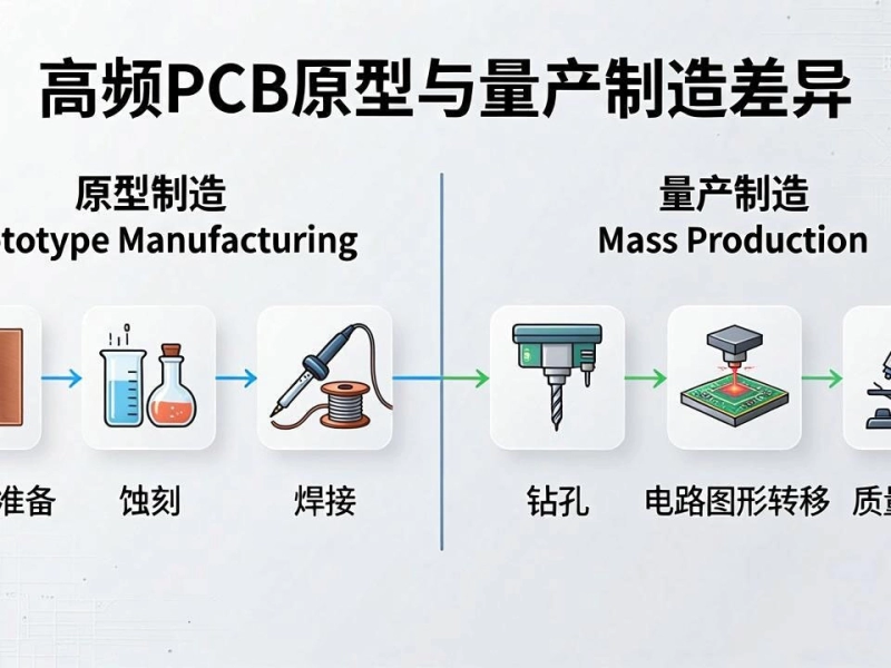
High Frequency PCB Prototype vs. Mass Production: Key Differences in FabricationJune/05/2026