As global Telecommunications Infrastructure races toward 6G technology, the demand for cutting-edge High Frequency Pcb Capabilities has never been more critical. While 5G networks continue their worldwide rollout, researchers and engineers are already pushing the boundaries of what's possible in RF and Microwave Circuit Design.
6G promises unprecedented data rates, sub-millisecond latency, and connectivity that spans from autonomous vehicles to embedded sensors in everyday objects. But these ambitious goals require advanced PCB technologies that can reliably operate at millimeter-wave and terahertz frequencies—frequencies that challenge the fundamental limits of traditional circuit board materials and manufacturing processes.
This article explores our latest developments in high frequency Pcb Manufacturing specifically designed for 6G research applications. From advanced substrate materials to precision fabrication techniques, we'll examine how modern PCB technology is enabling the next generation of wireless communication.
The transition from 5G to 6G represents more than just an incremental improvement in speed. It involves fundamental shifts in the electromagnetic spectrum used for communication, with 6G systems expected to operate in frequency bands ranging from 7 GHz to beyond 300 GHz.
At these elevated frequencies, conventional Pcb Materials introduce significant performance limitations:
Our 6G research PCBs address these challenges through carefully engineered material systems and manufacturing processes optimized for millimeter-wave performance.
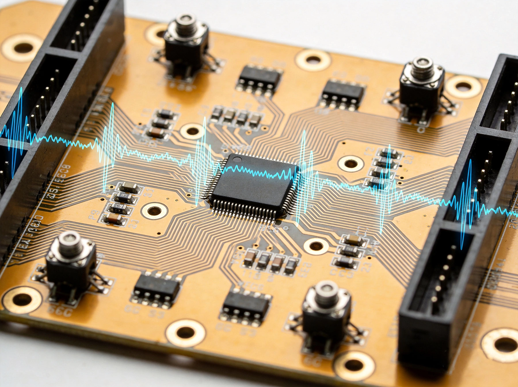
The foundation of any Rf Pcb is its substrate material. For 6G research applications, we work with specialized high-frequency laminates that provide superior electrical performance.
Rogers Corporation materials remain the gold standard for high-frequency applications:
For the most demanding 6G research applications, we offer advanced ceramic-based substrates:
We're also investing in emerging material technologies:
High-frequency PCB performance depends not just on material selection but on fabrication precision. At millimeter-wave frequencies, even microscopic variations can dramatically impact circuit behavior.
Maintaining precise Impedance Control (±5% or better) requires:
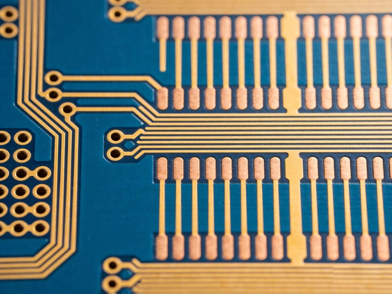
6G applications often require traces as narrow as 50-100 microns:
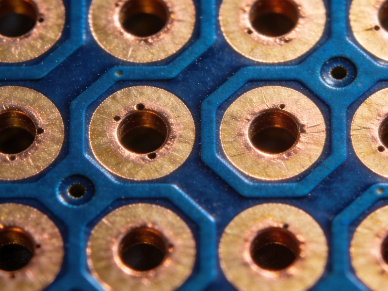
Rf Pcb vias present unique challenges at high frequencies:
As frequencies increase, traditional discrete component mounting becomes impractical. Our capabilities include advanced integrated packaging solutions for 6G research.
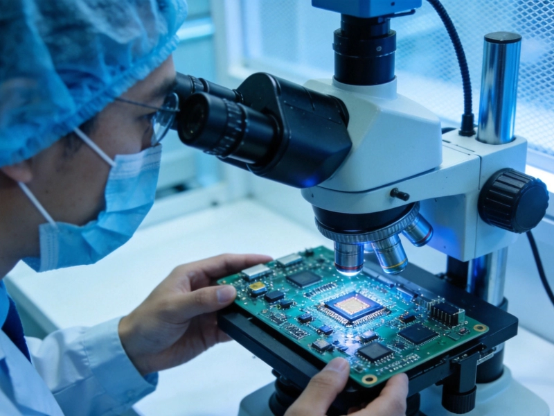
Designing high frequency PCBs for 6G research requires comprehensive testing capabilities. We maintain extensive RF characterization infrastructure to verify performance.
We provide comprehensive engineering support to help researchers optimize their high-frequency PCB designs:
6G research often requires small quantities of highly complex boards with rapid turnaround. Our manufacturing capabilities support:
Our High Frequency Pcb Capabilities support diverse 6G research applications:
6G will rely heavily on massive MIMO (Multiple Input Multiple Output) architectures with hundreds of antenna elements. Our PCBs enable:
High-frequency transceivers require sophisticated RF front-end modules:
Research facilities require sophisticated OTA testing infrastructure:
While 6G standards are still evolving, researchers are already exploring terahertz frequencies beyond 300 GHz. These extreme frequencies present even greater challenges:
Our continued investment in advanced PCB capabilities positions us to support these future research directions as they mature from laboratory curiosities to practical applications.
The transition to 6G technology demands unprecedented advances in High Frequency Pcb capabilities. From novel substrate materials to precision fabrication techniques, every aspect of Pcb Manufacturing must evolve to meet the challenges of millimeter-wave and terahertz frequencies.
Our commitment to advancing PCB technology for 6G research means continuous investment in materials, equipment, and expertise. Whether you're exploring massive MIMO architectures, developing millimeter-wave front-end modules, or pioneering terahertz communications, we have the capabilities and experience to support your research objectives.
The limits of high-frequency performance are being pushed further than ever before. Let us help you push them even further.

Why Advanced Testing Equipment Defines Top High Frequency PCB CapabilitiesJuly/07/2026

High Frequency PCB Capabilities for Aerospace and Defense ApplicationsJuly/17/2026

Our Latest High Frequency PCB Capabilities for 6G ResearchMay/29/2026
Understanding High Frequency PCB Capabilities: Line Width, Spacing, and Layer CountJune/28/2026

The Role of AI in Modern High Frequency PCB Manufacturing: Precision and EfficiencyJune/30/2026
Laser Drilling and Microvias in Modern High Frequency PCB FabricationJuly/07/2026
How to Vet a High Frequency PCB Manufacturer for 5G and Millimeter Wave ProjectsJuly/25/2026
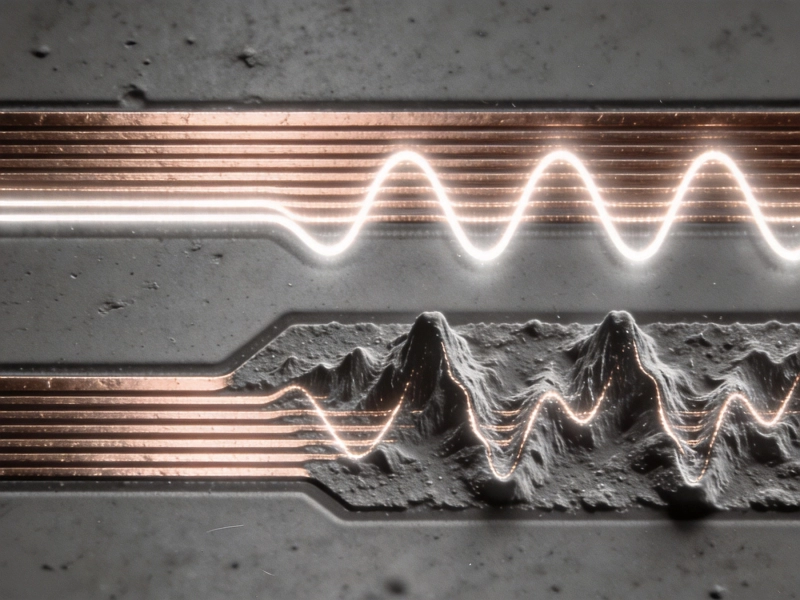
The Impact of Surface Roughness on High Frequency PCB Fabrication QualityJune/27/2026