Open Nav

Aerospace and defense systems operate at the cutting edge of high-frequency technology. Radar systems operating at X-band and Ka-band frequencies, Satellite Communications spanning multiple gigahertz, electronic warfare systems jamming across wide frequency spectrums — all depend on printed circuit boards that maintain Signal Integrity at frequencies where standard PCB technology fails completely.
Designing high-frequency PCBs for aerospace and defense requires expertise that goes beyond standard board design practices. The physics of high-frequency signal propagation, the electromagnetic environments military equipment must survive, and the reliability requirements for mission-critical systems all create unique design challenges. This guide explores the specialized capabilities and design approaches that make aerospace and defense high-frequency PCBs possible.

Understanding the frequency ranges your application operates in is the starting point for High-frequency Pcb design. Aerospace and defense systems operate across a wide spectrum, and each frequency range creates different design requirements.
Radar systems operate at frequencies from 8 GHz (X-band) through 110 GHz (W-band) depending on application. X-band radar at 8-12 GHz provides weather monitoring and air traffic control capabilities. Ku-band (12-18 GHz) and Ka-band (26-40 GHz) radar provide higher resolution for terrain mapping and precision targeting. Millimeter-wave radar at 60 GHz and beyond enables automotive adaptive cruise control and industrial sensing.
At these frequencies, wavelength becomes small enough that board dimensions and trace geometry matter. A 100 mil trace at 30 GHz is approximately a quarter-wavelength, meaning trace length itself becomes a Transmission Line characteristic rather than an approximate connection between components. Board stack-up thickness becomes meaningful in terms of electrical length, and even small physical deviations become significant phase errors.
Satellite Communications span from L-band (1-2 GHz) for mobile satellite service through Ka-band (26-40 GHz) for high-throughput satellite internet. Ka-band systems provide multi-gigabit-per-second throughput but require precise control over phase and amplitude characteristics that demand exceptional PCB consistency and repeatability.
Phase linearity across wide bandwidths becomes a critical requirement. A phase variation of 2-3 degrees across a 500 MHz Ka-band channel can degrade constellation diagrams and increase bit error rates. PCB Dielectric Constant variation across temperature and frequency directly impacts phase performance, making material selection and process control essential.
Electronic warfare systems monitor and jam across extremely wide bandwidths, often from DC frequencies up to 50 GHz or higher. These systems require PCBs that maintain consistent performance across multiple decades of frequency while simultaneously providing Shielding, isolation, and signal routing that prevents system self-interference.
The wide bandwidth requirement creates material selection challenges because dielectric properties vary with frequency. A material that performs well at 1 GHz may have significantly different properties at 20 GHz. This variation makes Impedance Control difficult across wide bandwidths and requires careful characterization of material frequency-dependent behavior.
Pcb Materials for aerospace and defense high-frequency applications differ substantially from standard FR4 used in commercial electronics. Low Dielectric Constant, low loss tangent, and tight material property control are essential requirements.
Dielectric constant (Dk) determines the speed of signal propagation through the material. Lower Dk signals propagate faster and with less wavelength compression, allowing larger physical dimensions for given electrical lengths. For high-frequency designs, lower Dk (typically 2-4) is preferred to maintain reasonable trace widths for given impedance requirements.
Loss tangent (Df) quantifies how much signal energy dissipates as heat as signals propagate. At high frequencies, loss tangent matters exponentially because losses increase with frequency. Standard FR4 has loss tangent around 0.02, which becomes unacceptable above a few gigahertz. High-frequency materials have loss tangents typically below 0.003, with some materials reaching below 0.001 for millimeter-wave applications.
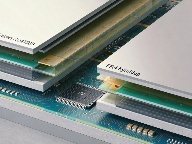
The trade-off is cost — materials with low Dk and low Df cost significantly more than FR4. For applications with mixed frequency requirements, hybrid stack-ups using both low-loss and standard materials can reduce cost while maintaining performance where it matters.
Aerospace and defense applications demand material property consistency from board to board and across production runs. Dielectric constant variation of ±5% might be acceptable for commercial products, but aerospace systems often require ±1% or better to maintain phase accuracy and Impedance Control.
This consistency requires tight material specifications from suppliers and process control during board fabrication. Even with tight specifications, actual dielectric constant can vary between production lots. Designers must account for this variation in their designs by specifying tolerances that accommodate expected material variation.
Aerospace and defense equipment experiences temperature extremes from -55°C in high-altitude or space environments to +125°C in under-hood avionics. Dielectric properties change with temperature, affecting impedance and phase characteristics. Materials must maintain performance across the entire operating temperature range.
Some materials provide thermal compensation that stabilizes dielectric constant across temperature ranges. These materials cost more but simplify temperature compensation designs. For critical applications, consider materials with specified temperature coefficients of dielectric constant that allow compensation calculations.
At high frequencies, copper conductivity becomes increasingly important because conductor losses dominate over dielectric losses. Standard electrodeposited copper typically provides sufficient conductivity, but at very high frequencies (30 GHz+), rolled annealed copper with smoother surfaces reduces Skin Effect losses.
Copper Surface Roughness becomes significant at high frequencies because the skin depth becomes small enough that surface roughness creates additional resistance. Smooth copper foils reduce this effect but cost more and may require special bonding techniques during lamination.
How you stack and configure PCB layers determines Signal Integrity at high frequencies. The layer count, material selection for each layer, and layer sequencing all affect performance.
High-frequency boards typically have higher layer counts than equivalent low-frequency designs because Controlled Impedance signals require dedicated reference planes and because routing density demands more routing layers. Ten to twenty layers are common for complex aerospace high-frequency designs.
Symmetric stack-ups with even layer counts reduce warpage and maintain flatness through thermal cycling. Symmetry also balances mechanical stresses, which matters for boards that experience temperature cycling in aerospace environments. When asymmetric stacks are unavoidable, compensate with thickness variations that maintain overall balance.
Dedicated ground planes adjacent to every signal layer provide Return Current paths that maintain impedance control and reduce radiation. At high frequencies, Return Current follows the path of least impedance, which for high-speed signals is the adjacent Ground Plane directly under the trace. Without adjacent ground planes, return currents find alternative paths creating unpredictable impedance and increased electromagnetic emissions.
Power planes should be placed adjacent to ground planes where possible to create decoupling capacitors through the plane capacitance. This plane capacitance provides high-frequency decoupling more effectively than discrete capacitors because it has very low inductance.
Not all layers in a hybrid stack-up need use the same materials. Signal layers routing high-frequency signals require Low-loss Materials, but layers routing low-speed control signals or power distribution can use less expensive materials. Strategic material assignment reduces cost while maintaining performance where required.
For example, a 12-layer board might use Rogers 4350B for the four outer signal layers carrying high-frequency RF signals, while the inner layers use standard FR4 for power distribution and low-speed digital routing. This hybrid approach provides high-frequency performance without the cost of full-stack Low-loss Materials.
Vias create discontinuities in Transmission Lines that cause impedance mismatches and reflections at high frequencies. Every via transition should include compensation structures like anti-pads, ground stitching, or via back-drilling to minimize discontinuities.
Via back-drilling removes the unused portion of plated through-holes, eliminating stubs that create resonances and impedance mismatches. Back-drilling adds process cost but is essential for signals above 10 GHz or in applications requiring exceptionally consistent performance.
Maintaining signal integrity at high frequencies requires attention to Transmission Line design, termination, and routing practices that low-frequency designs can ignore.
All high-frequency signals require Controlled Impedance routing. The impedance value (50 ohms single-ended or 100 ohms differential for aerospace applications) must be maintained within tight tolerances across manufacturing variation. Impedance tolerances of ±5% are common for high-frequency designs, with some applications requiring ±3% or better.
Impedance calculation requires accurate knowledge of dielectric constant, dielectric thickness, copper thickness, and trace geometry. Designers typically provide impedance specifications to PCB fabricators who then calculate trace widths and spacings required to achieve target impedances using their specific material lots and process capabilities.
Microstrip traces on outer layers are easy to probe and modify but expose signals to external interference and create radiation. Stripline traces between ground planes provide Shielding but are harder to probe and require internal routing. Coplanar waveguide structures provide good control over impedance and excellent isolation but consume more routing space than other structures.
Choose transmission line type based on isolation requirements, routing density needs, and maintainability considerations. Many aerospace designs use a combination of structures — Microstrip for easily testable signals, stripline for sensitive high-frequency routing, and coplanar waveguide for critical RF paths.
All high-frequency signals must be properly terminated to prevent reflections that distort signals. Source termination, end termination, or both may be required depending on signal frequency and routing length. Transmission Lines longer than approximately one-tenth wavelength generally require termination to prevent reflection problems.
Matching networks may be required at source or destination interfaces to compensate for impedance mismatches caused by connectors, component packages, or other discontinuities. These matching networks often use distributed elements (stubs, transmission line transformers) rather than lumped components to maintain high-frequency performance.
At high frequencies, electric and magnetic fields couple energy between adjacent traces, creating crosstalk that can degrade signal quality. Maintain 3x trace width spacing between parallel traces where possible, and provide ground traces between critical signals and other traces when closer spacing is unavoidable.
Differential pairs should maintain consistent spacing throughout their routing length. Any deviation from the specified differential spacing changes the differential impedance and creates mode conversion problems. Route differential pairs together and maintain equal length to within tight tolerances (typically 5 mil or less) for high-frequency signals.
Aerospace and defense equipment operates in electromagnetically challenging environments. The PCB itself must provide shielding and isolation to prevent external interference from affecting sensitive circuits and to prevent internal circuits from radiating excessively.
Board-level shielding cans isolate sensitive circuits from external electromagnetic fields. These shields typically consist of metal enclosures soldered to the PCB Ground Plane, creating a Faraday cage around protected circuitry. Shield effectiveness depends on material, seam sealing, and aperture size.
Design shields with minimal apertures and ensure good electrical contact between shield and ground. Apertures required for connectors or cables should be filtered or designed to maintain shielding effectiveness. Use finger stock or gaskets to maintain electrical continuity across shield seams.
Proper Grounding provides both signal return paths and shielding effectiveness. Star Grounding schemes avoid creating ground loops that pick up interference. Isolate ground planes where necessary to prevent coupling between circuits with different noise characteristics.
For systems with both analog and digital circuitry, separate the grounds and connect them at a single point to prevent digital noise coupling into sensitive analog sections. The connection point should be chosen based on current return paths rather than arbitrarily.
External interfaces require filtering to prevent conducted Electromagnetic Interference from entering or leaving the board. Place filters at connector interfaces where external cables attach, using pi filters, common-mode chokes, or ferrite beads as appropriate for the interface frequency range.
Isolate noisy power supplies and clock generators from sensitive Rf Circuits using power plane splits or local filtering zones. These isolation zones should have their own ground connections and decoupling to prevent noise coupling.
High-frequency components dissipate significant power, and signal losses at high frequencies convert to heat that must be managed to maintain performance and reliability.
Power amplifiers, LNAs (low-noise amplifiers), and frequency synthesizers in high-frequency systems dissipate substantial power. Provide adequate thermal paths from these components to heat sinks or thermal spreaders using thermal vias and copper pours.
Thermal vias under high-power components create low-resistance thermal paths to internal ground planes or backside heat spreaders. Fill these vias with thermally conductive material and plate them flush to provide maximum thermal conductivity.
Signal losses in the dielectric material create heat distributed across the board, not just concentrated at components. This distributed heating creates temperature gradients that affect dielectric constant and create mechanical stress from thermal expansion mismatch.
Estimate total Signal Loss for all high-frequency signals and convert to heat generation. This calculation helps identify Thermal Management requirements that might not be obvious from component power dissipation alone.
Components soldered to large copper planes require thermal relief pads to prevent heat sinking during soldering that would create cold solder joints. These thermal relief features reduce the thermal connection between the pad and the plane during assembly but still provide adequate thermal conduction during operation.
Balancing thermal relief needs with high-frequency performance requires careful design. Thermal relief traces create inductance that affects high-frequency performance. Use enough thermal relief features to enable assembly while maintaining electrical performance requirements.
High-frequency PCBs require specialized testing beyond standard electrical tests to validate performance and reliability for aerospace and defense applications.
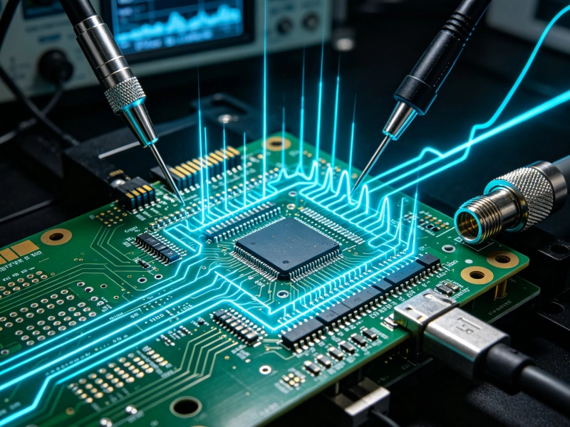
Vector network analyzers (VNAs) measure S-parameters that characterize transmission and reflection characteristics. S11 (return loss), S21 (Insertion Loss), and S22 (output return loss) measurements verify Impedance Matching and transmission line performance. Differential measurements verify balance in differential pairs.
Vna measurements typically span multiple octaves of frequency to validate performance across the full operating range. Measurements should be performed on multiple production samples to verify consistency across manufacturing variation.
Tdr measurements locate impedance discontinuities along transmission lines. Tdr generates a fast edge and measures reflections, displaying impedance versus distance along the trace. This technique identifies mismatches caused by vias, connectors, or routing problems that aren't apparent from S-parameter measurements.
TDR is particularly valuable for debugging production problems because it identifies physical locations of discontinuities. When a board fails high-frequency testing, TDR can pinpoint whether the problem is at a connector, via transition, or along trace routing.
Aerospace and defense boards must survive and operate through environmental extremes. Thermal cycling from -55°C to +125°C validates material stability and mechanical reliability. Vibration testing ensures the board survives mechanical stresses encountered in aircraft, missiles, or satellites.
Combined environmental tests that apply thermal stress while operating the high-frequency circuitry catch interaction effects that single-stress tests miss. A board that passes vibration testing at room temperature might fail at elevated temperature where material properties change.
Aerospace and defense applications have reliability requirements far more demanding than commercial products. Boards must operate through years of service with minimal failure probability and must be maintainable when service is required.
FMEA (Failure Modes and Effects Analysis) systematically examines potential failure modes and their consequences. For high-frequency PCBs, failure modes include thermal degradation of dielectric properties, mechanical failure at via transitions, solder joint fatigue under thermal cycling, and connector degradation.
Design mitigations for identified failure modes include redundancy, derating, and monitoring. Redundant signal paths provide alternate routing options if primary paths fail. Derating means designing components and circuits to operate well below their maximum ratings to increase reliability margins.
MTBF (Mean Time Between Failures) requirements for aerospace and defense systems often exceed 50,000 hours of operation. Achieving these requirements requires careful component selection, derating, and design practices that minimize stress on components and interconnections.
High-frequency components should be selected for established aerospace or military qualification. Components without qualification history should undergo accelerated life testing to establish failure rates before deployment.
While boards in some aerospace applications are designed to be replaced rather than repaired (spacecraft satellites, for example), many defense applications require field service capability. Repair considerations include component accessibility, rework difficulty, and test point availability for fault isolation.
High-frequency boards often use components with lead pitches that are difficult to rework. Provide adequate clearances for rework tools, specify rework procedures, and consider whether repairability requirements justify larger component packages or alternative assembly methods.
High-frequency Pcb technology continues advancing as aerospace and defense applications push toward higher frequencies and more complex systems. Emerging trends include millimeter-wave frequencies above 100 GHz, integration of antennas directly on PCBs, and materials with even lower loss characteristics.
Applications like Automotive Radar and high-throughput satellite communication push toward millimeter-wave frequencies above 60 GHz. At these frequencies, conventional PCB approaches reach their limits, and specialized techniques like substrate-integrated waveguides (SIW) provide alternative signal routing methods.
SIW structures create waveguide-like behavior using rows of vias to form sidewalls, providing low-loss signal routing without requiring machined metal waveguides. These structures integrate directly into PCB stack-ups, allowing planar fabrication of what would otherwise require complex mechanical assembly.
Integrating antennas directly onto PCBs reduces size and eliminates external antenna feeds. Patch antennas, slot antennas, and more complex antenna arrays can be fabricated directly on PCB layers, enabling compact radar and communication modules.
Antenna integration requires careful control of dielectric constant and thickness because these parameters directly affect antenna frequency and radiation characteristics. The same material consistency requirements that apply to transmission lines also apply to antenna performance.
Materials development continues pushing toward lower loss tangents, improved temperature stability, and better mechanical properties. Materials with Df below 0.001 are becoming commercially available, enabling higher frequencies and longer transmission lines than previously possible.
Hybrid materials combining low-loss dielectric with FR4 layers provide cost optimization. Advanced manufacturing techniques like laser direct imaging enable finer features and tighter tolerances, supporting higher frequencies and more dense designs.
High-frequency PCB capabilities for aerospace and defense require attention to every aspect of design — from material selection through stack-up configuration to shielding and testing. The physics of high-frequency signal propagation means that details that don't matter at low frequencies become critical design considerations.
Start with clear understanding of frequency requirements. Different applications operate at different frequencies with different performance requirements. Radar systems have different needs than satellite communications, which differ from electronic warfare. Match your design to the specific frequency ranges and performance criteria of your application.
Material selection sets fundamental performance limits. Low dielectric constant, low loss tangent, and tight material property control are essential requirements. Hybrid stack-ups can reduce cost by using high-performance materials only where needed. Choose materials that maintain performance across the full operating temperature range.
Stack-up design provides the foundation for signal integrity. Symmetric constructions reduce warpage and maintain flatness. Dedicated ground planes provide return current paths and shielding. Strategic material assignment optimizes cost versus performance. Careful via design minimizes discontinuities.
Signal integrity design techniques maintain signal quality through controlled impedance, proper termination, and careful routing. Every transmission line should be designed as a deliberate structure rather than an accidental routing choice. Crosstalk reduction becomes increasingly critical as frequencies increase.
Emc and shielding strategies prevent interference both entering and leaving the board. Board-level shielding cans isolate sensitive circuits. Proper grounding provides both signal return paths and shielding. Filtering at interfaces prevents conducted interference.
Testing validates that designs meet requirements. Network analysis measures S-parameters across frequency ranges. TDR locates impedance discontinuities. Environmental testing validates operation through thermal and mechanical stress. Testing should span multiple production samples to verify consistency.
Reliability engineering ensures boards survive years of service. FMEA identifies potential failure modes and designs mitigations. MTBF requirements influence component selection and derating. Maintainability considerations determine field service capability.
High-frequency PCB capability for aerospace and defense isn't about individual design tricks — it's about systematic attention to all aspects of design, manufacturing, and testing. When every detail receives appropriate attention, the resulting boards provide the performance and reliability that aerospace and defense systems demand.
Rogers 4350B (Dk ~3.48, Df ~0.0037) and RT/Duroid 5880 (Dk ~2.2, Df ~0.0009) are widely used for aerospace high-frequency applications. These materials provide good balance of performance, manufacturability, and cost. For millimeter-wave applications above 60 GHz, materials like Rogers 3003 with even lower loss tangents become attractive. Hybrid stack-ups combine these materials with standard FR4 for cost optimization.
Tight impedance control requires accurate material property characterization, careful stack-up design, and process control during fabrication. Provide impedance specifications to your Pcb Manufacturer, who will calculate trace dimensions using their specific material lots. Specify impedance tolerance requirements clearly (±5% for many applications, ±3% for critical paths) and verify with TDR or Vna measurements on first-article production boards.
Microstrip routes signals on outer layers with a single reference plane below, providing easy access for probing and modification but exposing signals to external interference. Stripline routes signals between two reference planes, providing excellent shielding but making probing and modification difficult. Stripline typically has lower loss and better isolation but requires careful control of layer thickness to maintain impedance. Choose based on isolation requirements, accessibility needs, and routing density.
Transitions between different transmission line types (microstrip to stripline, stripline to connector) require compensation structures to minimize impedance discontinuities. Use via back-drilling to remove stubs. Implement ground stitching vias adjacent to signal vias to provide continuous return paths. Design anti-pads with appropriate sizing to control capacitance. Model transitions in Em Simulation software and verify with TDR measurements on prototype boards.
Standard testing includes VNA measurements of S-parameters (S11, S21, S22) across the operating frequency range. TDR measurements locate impedance discontinuities. Time domain measurements verify signal integrity with actual signals. Environmental testing validates performance through temperature and vibration stress. For production, implement 100% electrical testing plus statistical sampling of RF performance to verify consistency.
High-frequency PCB capability enables aerospace and defense systems that were impossible a generation ago. As frequencies continue increasing and system complexity grows, the design principles outlined here provide the foundation for next-generation high-frequency electronics that meet the demanding requirements of aerospace and defense applications.
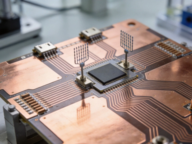
A Deep Dive into High Frequency PCB Capabilities for Millimeter Wave TechSeptember/24/2026
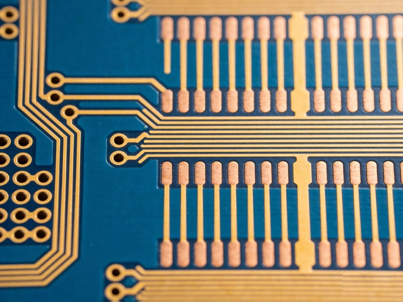
Understanding High Frequency PCB Capabilities: Line Width, Spacing, and Layer CountJune/28/2026

Why Advanced Testing Equipment Defines Top High Frequency PCB CapabilitiesJuly/07/2026
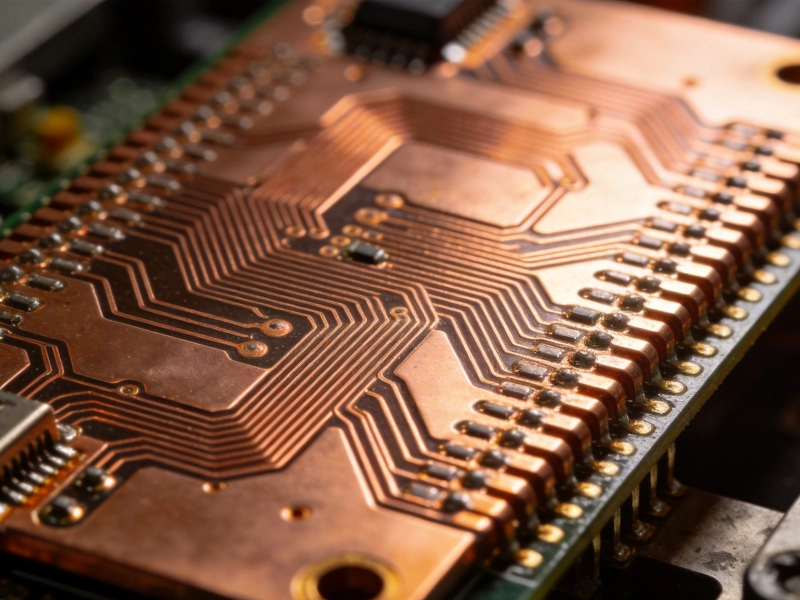
High Frequency PCB Capabilities: Handling Thick Copper and High Power RFSeptember/15/2026
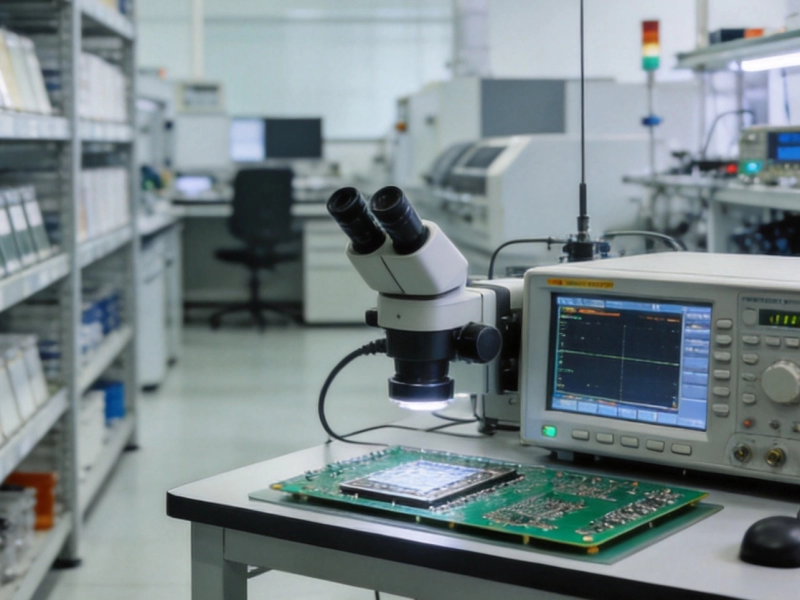
Upgrading Your Supply Chain with Our Expanded High Frequency PCB CapabilitiesOctober/09/2026

Our Latest High Frequency PCB Capabilities for 6G ResearchMay/29/2026
Exploring Our High Frequency PCB Capabilities in Mixed Material LaminationJuly/29/2026
The Importance of Impedance Control in Our High Frequency PCB CapabilitiesSeptember/03/2026