Open Nav

As wireless communication systems push into higher frequency spectrums—5G mmWave, Automotive Radar at 77GHz, Satellite Communications above 10GHz—the humble printed circuit board has evolved into a precision engineering component where every microscopic detail affects Signal Integrity. At the heart of this evolution lies laser drilling technology and the microvia, enabling circuit densities and electrical performance that mechanical drilling simply cannot achieve.
This article explores the technical foundations, manufacturing processes, and practical considerations that engineers and procurement specialists need to understand when working with laser-drilled microvias in high-frequency PCB Fabrication.
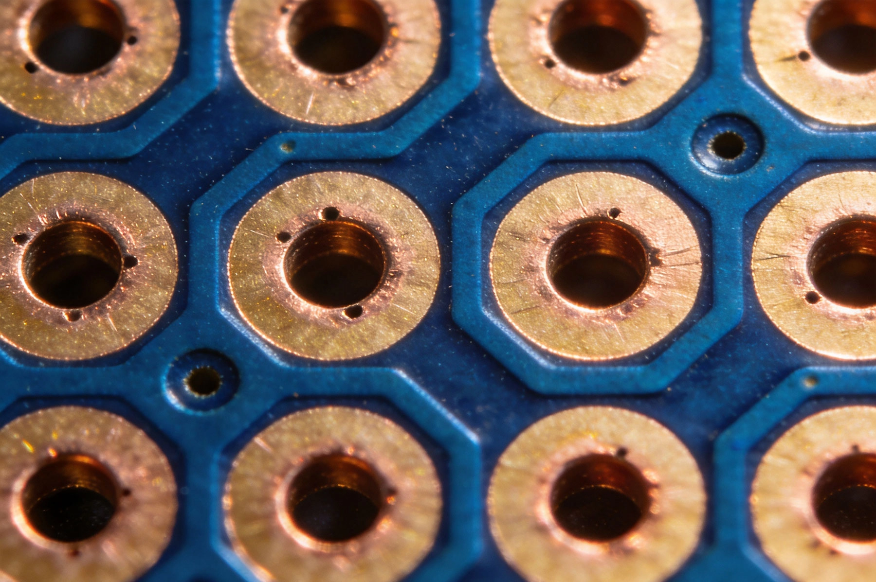
The term "microvia" encompasses any via with a diameter significantly smaller than traditional mechanically drilled holes. While definitions vary across the industry, microvias typically refer to holes ranging from 25 to 150 micrometers in diameter—dimensions measured in fractions of a human hair.
To appreciate why microvias matter for high-frequency applications, consider what happens to a signal traveling through a via. Every via creates an impedance discontinuity—a disruption in the Controlled Impedance pathway that Signal Integrity engineers work so hard to maintain. Smaller vias mean shorter stub lengths, reduced parasitic capacitance, and less signal distortion. At frequencies above 10GHz, these seemingly minor factors determine whether a design functions or fails.
Beyond electrical performance, microvia technology enables the layer-to-layer interconnect densities required by modern semiconductor packaging. Ball Grid Array (BGA) packages with 0.4mm and 0.5mm pin pitches demand via capture pad diameters that mechanical drills simply cannot achieve reliably. The transition to microelectronics has made laser drilling not just advantageous but essential.
Laser drilling employs concentrated light energy to remove material from the PCB substrate, creating precise holes without physical contact or mechanical stress. Two primary laser technologies dominate PCB Fabrication: CO2 lasers and UV lasers, each offering distinct advantages.
CO2 Laser Drilling
Carbon dioxide lasers emit infrared radiation at 10.6 micrometers wavelength, efficiently absorbed by organic materials like epoxy and polyimide but reflected by copper. This characteristic makes CO2 lasers ideal for drilling blind vias in dielectric layers—laser energy passes through copper foil to ablate the underlying substrate, then a subsequent desmear process removes any copper smear created during drilling.
CO2 lasers achieve drilling speeds of 200 to 1000 holes per second, making them economically viable for high-volume production. Hole quality is excellent, with typical wall angle tolerances of 70-85 degrees, suitable for most sequential lamination processes. The technology handles a wide range of substrate thicknesses and can produce reliable blind vias in boards with 4 to 12 mil dielectric layers.
UV Laser Drilling
Ultraviolet lasers operating at 355nm or 266nm wavelengths offer fundamentally different capabilities. UV energy is absorbed by copper, making these lasers suitable for drilling through copper foils directly without the dielectric-only restriction of CO2 systems. This enables true microvia formation in copper-clad laminates.
UV laser drilled holes exhibit superior geometry—wall angles approaching 88-90 degrees produce virtually vertical sidewalls. This characteristic becomes critical for high-density interconnect (HDI) boards where via-in-pad and stacked microvia architectures demand precise dimensional control. The tradeoff is slower throughput: UV systems typically drill 50 to 300 holes per second, justifying premium pricing only for the most demanding applications.
Creating reliable microvias involves more than simply drilling holes. The process unfolds across multiple stages, each contributing to final via quality and reliability.
Microvia formation begins before drilling commences. Panel preparation includes cleaning to remove organic contamination, micro-etching to ensure proper copper adhesion, and sometimes copper thickness reduction to achieve the thin copper requirements for laser drilling. For sequential lamination builds, inner layer circuitization must be complete and verified before outer layer processing proceeds.
The copper surface condition significantly affects laser drilling performance. Excessive oxidation, contamination, or uneven copper distribution can cause inconsistent drilling depth and quality. Reputable fabricators maintain strict incoming inspection and surface preparation protocols to ensure consistent starting conditions.
Drilling parameters require careful optimization for each substrate type, copper weight, and target via geometry. Key parameters include:
Pulse energy determines the amount of material removed per laser pulse. Too little energy produces incomplete ablation; too much causes thermal damage to surrounding material and creates HAZ (Heat Affected Zone) that compromises dielectric integrity.
Pulse overlap controls the spacing between successive laser pulses. Higher overlap produces smoother hole walls but requires more pulses per hole, increasing cycle time. Finding the optimal overlap balances quality against throughput for each product family.
Number of hits determines total drilling depth for blind vias. CO2 lasers typically require multiple hits to penetrate through-hole blind via depths, with each hit removing a specific depth increment. The cumulative effect produces the tapered geometry characteristic of CO2-drilled blind vias.
Repetition rate—the frequency of laser pulses—affects both drilling speed and heat accumulation. Modern laser systems dynamically adjust repetition rates throughout the drilling program to optimize quality across varying feature densities.
Following laser drilling, a desmear process removes residual epoxy smear from via walls and from barrel surfaces. For CO2-lased blind vias, this step is essential because the laser heat partially melts and redeposits epoxy on copper surfaces, creating non-conductive films that prevent proper plating adhesion.
Plasma desmearing using oxygen and nitrogen gas mixtures has largely replaced chemical desmear processes in modern fabrication. Plasma treatment offers superior consistency, Environmental Compliance, and the ability to adjust desmear aggressiveness for different substrate materials.
After desmear, via metallization proceeds through standard electroless and electroplating processes. For microvias, conformal copper coverage demands precise control of plating parameters to achieve uniform barrel thickness throughout the via depth. Typical specifications require 25-30 micrometers minimum copper thickness on via walls for reliable thermal cycling performance.
High-frequency Pcb designs increasingly employ advanced microvia architectures that push the boundaries of fabrication capability.
Via-in-Pad (VIP) technology routes vias directly into component pad areas, eliminating the annular ring requirement and recovering significant board real estate. For dense BGA packages, VIP enables tighter routing pitch and reduces overall board size. The technique requires careful copper plating control and often employs plug-and-plate processes to create flat pad surfaces for component mounting.
Stacked microvias—directly stacked on top of each other through sequential lamination layers—enable vertical interconnect densities impossible with traditional through-hole technology. A 12-layer HDI board might incorporate three or four stacked microvia structures, creating dense signal routing pathways that dramatically reduce board area requirements.
Caution accompanies these advanced techniques. Stacked via reliability depends critically on plating quality and lamination void elimination. Designs incorporating stacked microvias should specify thermal cycling requirements, and fabricators should qualify these structures through accelerated stress testing before committing to production volumes.
For RF and microwave applications, microvia design involves electrical performance tradeoffs that differ from digital signal routing concerns.
Via stub length—the non-functional portion of a via extending below the signal layer—creates parasitic capacitance that degrades high-frequency performance. In mmWave applications above 30GHz, even 100-micrometer stubs can introduce measurable impedance discontinuities. Design techniques to minimize stub effects include:
Back-drilling removes the non-functional barrel portion of through-hole vias, eliminating stubs for layer-specific routing. While technically different from microvia fabrication, back-drilling achieves similar signal integrity benefits for high-frequency differential pairs and critical RF traces.
Blind and buried via placement directly connects only the layers that carry signals, eliminating unnecessary stub length from the circuit entirely. This technique requires precise stack-up design and lamination control but delivers superior high-frequency performance.
Via fencing—ground vias placed adjacent to signal vias—helps control electromagnetic field distribution and reduces crosstalk between adjacent signal routes. At high frequencies, the coupling between nearby vias becomes significant, making via planning as important as trace routing.
Not all PCB substrates respond equally well to laser drilling. Material characteristics fundamentally affect drilling speed, hole quality, and process reliability.
Standard Fr-4 Epoxy/Glass
Conventional Fr-4 laminates, while excellent for standard PCB applications, present challenges for microvia fabrication. The glass reinforcement weave creates inconsistent laser absorption, potentially causing incomplete ablation in areas where resin content varies. Fabrics typically recommend FR-4 with special laser-rated formulations that ensure more uniform drilling characteristics.
Polyimide Films
Polyimide substrates—commonly used in flex and rigid-flex circuits—respond exceptionally well to laser drilling. The homogeneous material composition produces consistent ablation rates and clean hole walls. Polyimide's thermal resistance also withstands the heat input from laser processing without degradation.
High-Frequency Laminates
Rf Materials like Rogers RT/duroid, Taconic RF substrates, and Arlon Ptfe composites present unique challenges. Ptfe's low dielectric loss makes it ideal for high-frequency applications but complicates laser processing. The material's thermal properties require careful parameter optimization to achieve clean ablation without thermal damage. Some PTFE laminates incorporate ceramic fillers that further complicate laser processing, sometimes requiring pre-treatment or modified approaches.
Hybrid stack-ups—combining FR-4 prepregs with high-frequency materials—introduce additional complexity. Laser drilling parameter transitions between material types demand process controls that ensure reliable drilling across the entire board area.
Microvia quality cannot be verified through visual inspection alone. The microscopic dimensions and hidden structures require sophisticated analysis techniques.
Cross-Section Analysis
Physical cross-sections through representative sample vias provide definitive verification of wall angle, plating thickness, and lamination interface integrity. This destructive test technique, while not suitable for 100% inspection, establishes process capability and validates design rule compliance. Most fabricators provide cross-section documentation for new product qualifications.
Thermal Cycling and Reliability Testing
Accelerated thermal cycling tests vias to failure, establishing reliability margins for specific stack-ups and via geometries. IPC standards provide guidance on test conditions and acceptance criteria, though many high-frequency applications require extended testing beyond standard requirements to ensure mission-life reliability.
Automated Optical Inspection Limitations
Standard AOI systems cannot penetrate below the surface to inspect microvia barrel quality. Acoustic micro-imaging (C-SAM) and X-ray Inspection provide internal quality verification that surface inspection cannot achieve. For critical applications, requesting these inspection techniques becomes essential for supply chain Quality Assurance.
Designing for microvia fabrication requires understanding both capabilities and limitations of the manufacturing process.
Via aspect ratio—the ratio of depth to diameter—constrains achievable geometries. Standard guidelines recommend maximum aspect ratios of 0.8:1 for CO2-lased blind vias, though advanced processes can achieve 1:1 ratios under controlled conditions. Deep microvia formation may require multiple drilling passes or alternative approaches like controlled depth laser ablation.
Pad size requirements depend on registration capabilities of the fabrication process. Standard guidelines recommend capture pad diameters of 3x the via diameter plus registration tolerance. For 75-micrometer microvias with 25-micrometer registration capability, this translates to pad diameters of approximately 250 micrometers.
Solder mask alignment becomes challenging when microvia capture pads approach solder mask registration tolerances. Via-in-pad designs require either plugged vias or solder mask tenting to prevent solder wicking into the via barrel during assembly. These options carry their own reliability implications that should be evaluated early in the design process.
Microvia technology carries cost premiums that must be weighed against performance benefits.
Laser drilling equipment represents significant capital investment—professional CO2 systems run $500,000 to $2 million, while UV laser systems can exceed $3 million. This investment amortizes across production volumes, making per-hole drilling costs highly dependent on order quantities. Small prototyping runs may show dramatically higher microvia costs than high-volume production runs.
The number of laser hits, drilling speed, and process complexity all affect microvia pricing. Stacked via architectures multiply process steps and inspection requirements, contributing to exponential cost increases for highly complex HDI structures.
Material selection also influences cost. High-frequency laminates like Rogers materials cost 5-10x more than standard FR-4, and their processing complexity often adds additional premiums. PTFE-based materials may require specialized laser processing parameters or alternative drilling techniques, further affecting pricing.
For high-frequency applications, these cost premiums often prove justified. The signal integrity benefits of microvia technology directly translate to product performance—better range for wireless systems, higher data rates for communication equipment, and improved radar resolution for automotive sensors. The engineering decision should focus on total cost of ownership, including development costs, field failure risks, and competitive positioning—not just fabrication quotes.
Microvia technology continues evolving alongside increasing demands from advanced semiconductor packaging and higher frequency applications.
Tape-based substrates using additive copper foil processes enable microvia formation on ultra-thin dielectrics, supporting the semiconductor industry's drive toward thinner and more compact packages. These technologies, while still emerging, point toward increasingly sophisticated interconnection solutions.
Direct imaging and laser direct structuring (LDS) approaches are being developed to combine microvia formation with additive patterning, potentially simplifying processes while enabling even finer feature resolution. These hybrid approaches blur traditional boundaries between subtractive and additive manufacturing.
Embedded component technologies increasingly integrate passive components within the PCB structure, reducing board area while eliminating surface mount assembly steps. Microvia technology supports these advanced packaging approaches by enabling dense vertical interconnection between embedded layers.
Not all PCB manufacturers possess equal microvia capabilities. Technical due diligence should evaluate several factors.
Equipment inventory reveals capabilities but doesn't guarantee performance. Ask about laser system maintenance practices, process control methodologies, and recent capability studies. A machine sitting idle may not deliver the quality of an actively maintained system.
Process capability documentation—statistical process control data, capability indices for critical dimensions, historical performance trending—demonstrates manufacturing maturity. Ask for Process Capability Index (Cpk) data for via dimensions and plating thickness distributions.
Material qualifications establish which substrate types the fabricator has successfully processed. A manufacturer may claim PTFE capability but lack specific experience with your target material. References from similar applications provide valuable validation.
Quality system certification—Iso 9001, AS9100 for aerospace, or IATF 16949 for automotive—indicates organizational commitment to quality processes. These certifications require regular audits and demonstrate systematic approaches to manufacturing control.
Laser drilling and microvia technology represent enabling capabilities that define modern high-frequency Pcb Fabrication. Understanding these technologies—whether you're designing Rf Circuits, specifying boards for procurement, or qualifying manufacturing partners—provides the foundation for successful high-performance electronic products. As communication systems continue pushing into higher frequency spectrums, microvia expertise will only grow in importance across the electronics industry.
The Impact of Surface Roughness on High Frequency PCB Fabrication QualityJune/27/2026
High Frequency PCB Fabrication with Rogers and PTFE Materials: A Technical GuideJuly/16/2026
Advanced High Frequency PCB Fabrication Techniques for Low Loss PerformanceMay/29/2026

Environmental Considerations in Sustainable High Frequency PCB FabricationSeptember/23/2026
High Frequency PCB Fabrication: Managing Dielectric Constant (Dk) TolerancesJune/09/2026
Hybrid Stack-ups: Combining FR4 and RF Materials in High Frequency PCB FabricationSeptember/14/2026
The Role of Vacuum Lamination in High Frequency PCB FabricationAugust/07/2026
Overcoming Delamination Challenges in Multilayer High Frequency PCB FabricationJuly/28/2026