
In the world of high-frequency printed circuit boards, the difference between adequate and exceptional manufacturing often comes down to a single question: how thoroughly can you measure what you've built? A manufacturer armed with a vector network analyzer and time-domain reflectometer can identify problems that remain invisible to anyone relying solely on basic continuity testing. This measurement capability doesn't just improve quality—it fundamentally defines what's possible in high-frequency PCB Fabrication.
As communication systems push into mmWave spectrums, Automotive Radar operates at 77GHz, and data center interconnects run at 56Gbps PAM4, the testing infrastructure behind Pcb Manufacturing has become the true arbiter of capability. Understanding why advanced testing equipment matters—and what separates genuine expertise from marketing claims—should be central to any procurement or engineering decision about High-frequency Pcb sourcing.
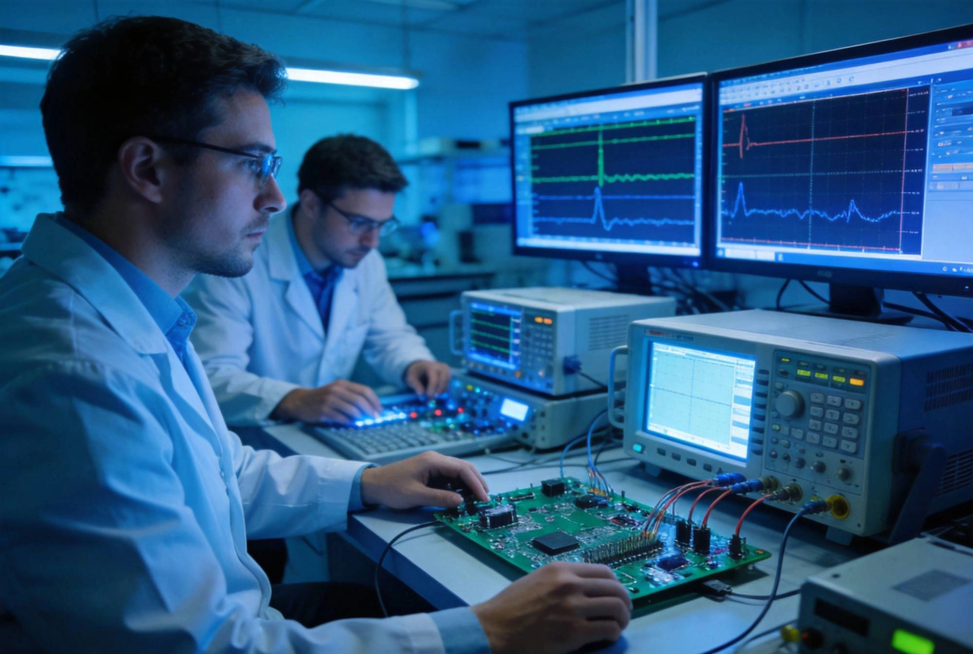
Electrical testing for standard digital circuits follows well-established rules. Continuity checks verify connections exist. Insulation resistance measurements confirm no unintended shorts. These tests, performed with basic equipment, adequately identify most manufacturing defects for boards operating at frequencies below 100MHz.
High-frequency Pcb behavior, however, follows different physics entirely. At 28GHz, a board that passes every continuity test might still fail catastrophically. Signal traces behave as Transmission Lines, with impedance controlled by trace geometry and dielectric properties. Via structures create impedance discontinuities that reflect signals. Dielectric losses accumulate with frequency, degrading signal strength in ways simple multimeters cannot detect.
The fundamental challenge is that high-frequency performance emerges from the interaction between materials, geometry, and manufacturing precision—factors that require correspondingly sophisticated measurement approaches to verify. Without advanced testing equipment, a manufacturer cannot know whether the board they built actually achieves the electrical specifications their customer requires.
The vector network analyzer (Vna) stands as the most critical instrument in high-frequency PCB characterization. A Vna transmits a swept-frequency signal into a device under test and measures how that signal is modified—how much power is reflected and how much is transmitted through. From these measurements, engineers extract S-parameters that fully characterize the device's frequency-dependent behavior.
For PCB fabricators, VNA measurements answer the questions that matter most. What is the Insertion Loss of a Transmission Line at 30GHz? How much return loss does a connector interface exhibit? What is the Characteristic Impedance of a trace geometry across the operating band? These parameters directly determine whether a PCB will function in the target application.
VNA capability specifications reveal significant capability differences. Frequency range determines which applications a system can address—a VNA covering DC to 40GHz cannot characterize 77GHz Automotive Radar circuits. Dynamic range—the difference between maximum signal and noise floor—limits the ability to measure low-loss structures accurately. Measurement accuracy depends on calibration techniques and reference plane establishment.
Top-tier PCB manufacturers operate VNA systems covering frequencies from 10MHz to 50GHz or higher, with dynamic range exceeding 100dB and measurement uncertainty below 0.1dB. These specifications are not marketing fluff—they directly translate to the ability to measure the increasingly demanding requirements of modern high-frequency applications.
While VNAs characterize frequency-domain behavior, time-domain reflectometry (Tdr) reveals how impedance varies along a trace's length. This capability proves essential for identifying localized discontinuities that degrade high-speed Signal Integrity.
A Tdr sends a fast-rise-time pulse down a Transmission Line and analyzes reflections returning from impedance changes. A perfect transmission line produces no reflections. An impedance bump—caused by geometric variation, plating inconsistency, or material inhomogeneity—creates a reflection proportional to the severity of the discontinuity.
For PCB Fabrication quality control, TDR analysis provides several irreplaceable capabilities. Single-ended and differential impedance measurements verify that trace geometries achieve target impedance values across production panels. Impedance uniformity mapping identifies process variations that might cause systematic performance degradation. Defect detection locates specific problem areas for failure analysis and process improvement.
Modern TDR systems achieve spatial resolution below 1mm, enabling identification of very small discontinuities. When combined with TDR-based impedance calculations, these instruments provide traceable measurements tied to physical trace geometry—critical for correlating fabrication processes with electrical specifications.
High-frequency PCB performance depends fundamentally on dielectric material properties. The Dielectric Constant (Dk) and loss tangent (Df) of the substrate determine trace impedance, propagation velocity, and signal attenuation. Variations in these properties—across the panel, from batch to batch, or with temperature—directly affect finished board performance.
Material characterization systems measure these properties using resonant or transmission-line techniques. Split-cylinder resonators extract Dk and Df from resonant frequency and quality factor measurements. Transmission-line methods characterize materials in simulated board configurations. These measurements require specialized fixtures, precise temperature control, and sophisticated analysis to achieve accurate results.
Leading PCB manufacturers maintain material characterization capabilities as part of their quality system. They verify incoming material properties against supplier specifications, monitor process consistency through production panel measurements, and validate that final boards meet the dielectric requirements their customers depend on. Without this capability, there's no way to know whether the expensive high-frequency laminate specified in the design actually delivered the expected electrical performance.
While electrical testing verifies performance, dimensional verification confirms that manufacturing processes produced geometry within specification. For high-frequency boards where trace width variations directly affect impedance, dimensional control becomes electrical performance control.
Automated optical inspection (AOI) systems image boards at high magnification, comparing manufactured features against design data. Modern AOI systems achieve resolution sufficient to measure trace widths at micron levels, identifying variations that could affect controlled-impedance performance. 3D measurement systems extend this capability to height measurements, verifying plating thickness, solder mask coverage, and Component Placement accuracy.
For high-frequency PCB manufacturers, AOI serves dual purposes. Defect detection identifies manufacturing flaws—opens, shorts, insufficient clearances—that would cause immediate failure. Process capability monitoring tracks dimensional distributions over time, enabling statistical process control that prevents out-of-spec production before it occurs.
High-frequency PCB applications often operate in demanding thermal environments. Automotive radar units experience temperature swings from -40°C to +125°C. Aerospace Electronics face similar extremes. These temperature variations stress solder joints, Dielectric Materials, and plated-through structures in ways that room-temperature electrical testing cannot predict.
Environmental stress testing evaluates how high-frequency PCB structures survive thermal cycling. Boards are cycled between temperature extremes while electrical measurements track performance changes. Signal Integrity degradation, impedance shifts, and interconnection failures all manifest through thermal stress testing—identifying reliability risks that wouldn't appear in standard electrical verification.
Top manufacturers maintain thermal cycling chambers capable of meeting relevant industry standards (IPC, MIL-PRF) and custom stress profiles matching specific application requirements. They document failure modes through detailed failure analysis, feeding insights back into process improvement. This testing capability separates manufacturers focused on meeting minimum specifications from those committed to delivering reliable performance throughout product life.
High-density interconnect structures—microvias, buried vias, and complex multilayer stacks—contain features that cannot be inspected optically. Plating quality inside microvia barrels, void content in solder joints, and delamination between layers all hide from external view, yet each represents a potential failure mechanism in high-frequency applications.
X-ray Inspection systems penetrate these structures, producing images that reveal internal features. 2D X-ray provides projection views showing overall void distributions and solder fill. 3D X-ray computed tomography reconstructs volumetric images enabling detailed analysis of internal structure integrity. These capabilities prove essential for qualifying complex HDI boards where internal features cannot be verified any other way.
Acoustic micro-imaging (C-SAM) provides complementary capabilities using ultrasonic waves. Different materials reflect ultrasound differently, enabling detection of delaminations, voids, and moisture ingress. The technique proves particularly valuable for identifying interface failures—between dielectric layers, within plated structures, or at material boundaries—that could cause field failures under thermal or vibration stress.
Manufacturers without these inspection capabilities cannot guarantee internal quality. They may ship boards with hidden defects that pass all external testing, only to fail in customer applications. For high-frequency boards where reliability requirements often exceed consumer electronics expectations, internal quality verification becomes non-negotiable.
Modern high-frequency PCBs often support digital signaling at speeds up to 56Gbps and beyond. At these data rates, signal integrity analysis extends beyond traditional RF measurements to include eye diagram analysis, jitter decomposition, and equalization verification.
High-speed digital testing employs sampling oscilloscopes with bandwidths exceeding 70GHz, enabling direct observation of fast-edged signals. Eye diagrams—superimposed bit patterns showing aggregate signal quality—provide intuitive visualization of link performance. Jitter measurement tools decompose total jitter into random and deterministic components, enabling prediction of bit-error-rate performance.
For PCB manufacturers, signal integrity testing serves two purposes. First, it validates that controlled-impedance traces meet Insertion Loss and impedance specifications at the data rates the board must support. Second, it provides correlation between material properties, fabrication processes, and finished board performance—enabling data-driven process optimization that improves quality continuously.
Understanding why testing equipment defines capability requires appreciating the capital investment involved. A professional-grade VNA suitable for characterizing 40GHz circuits costs $80,000 to $250,000. TDR systems with sufficient resolution add another $50,000 to $150,000. Material characterization systems, thermal chambers, X-ray equipment, and high-speed digital test systems each add comparable investments.
Full high-frequency Pcb Testing capability can easily represent $1 million to $3 million in capital equipment, plus specialized facilities, trained operators, and ongoing maintenance contracts. This investment does not generate revenue directly—it enables quality verification and process improvement that protect the manufacturer's reputation and their customers' product success.
Manufacturers who have made this investment demonstrate commitment to high-frequency PCB capability. Those who have not—who claim high-frequency expertise while outsourcing measurements to third-party labs or relying on basic electrical testing—cannot provide the verification their customers need. The equipment差距 is real, measurable, and fundamental to what separates capable manufacturers from those merely claiming to be.
When evaluating high-frequency PCB suppliers, the testing data they provide reveals much about their actual capabilities.
Impedance Measurement reports with full frequency-domain characterization demonstrate VNA capability. Look for S-parameter data showing insertion loss and return loss across the operating band, not just spot-frequency impedance values. TDR impedance profiles showing uniformity across trace lengths indicate process control. Material characterization data documenting Dk and Df measurements validates laminate verification practices.
The format and completeness of testing documentation matters equally. Professional manufacturers provide calibrated measurements with traceable uncertainty analysis. They include environmental conditions, calibration status, and measurement methodology. Reports with missing information, generic pass/fail indicators, or inconsistent formatting suggest quality systems that haven't matured to match their equipment.
Request actual measurement data from recent production—not promotional case studies or cherry-picked success stories. The willingness to share raw measurement results, even when they reveal marginal conditions, demonstrates confidence in both their processes and their measurement capability.
Measurement equipment only delivers value when properly calibrated against national standards. Calibration ensures that the numbers a VNA produces accurately represent the physical quantities being measured. Without traceable calibration, measurement results become meaningless regardless of instrument sophistication.
Professional PCB manufacturers maintain calibration programs meeting ISO 17025 requirements. They calibrate instruments against traceable standards at intervals determined by manufacturer recommendations and usage patterns. Calibration certificates document measurement uncertainty, environmental conditions during calibration, and reference standards used.
For customers, calibration documentation provides assurance that measurement results can be trusted. When a manufacturer claims 50-ohm impedance tolerance of ±5%, that claim only has meaning if the instruments making that measurement are properly calibrated. Ask about calibration programs and certificates—reluctance to provide this information suggests either missing capability or uncomfortable uncertainty about measurement accuracy.
Advanced testing equipment enables process control improvements that benefit both manufacturers and their customers. Without measurement capability, process improvement relies on trial and error—expensive, slow, and often misdirected. With measurement data, engineers can identify specific process variables that affect performance, enabling targeted optimization.
Statistical process control using electrical measurement data has transformed high-frequency Pcb Manufacturing. Manufacturers track impedance distributions across panels, monitoring for shifts that might indicate incoming material changes or equipment drift. They correlate plating process parameters with via impedance, optimizing plating chemistries for target electrical performance. They verify lamination pressure effects on Dielectric Constant, adjusting processes for different laminate types.
Customers benefit from this process maturity through more consistent quality, fewer surprises, and the ability to rely on specified performance across production volumes. When every board ships with measured electrical data confirming target specifications, procurement decisions become lower risk and Supply Chain Management simplifies.
Not all high-frequency testing capability is created equal. Several common gaps separate genuine expertise from marketing claims.
Frequency range limitations: A VNA covering 20GHz cannot characterize 28GHz or 77GHz circuits, regardless of what marketing materials claim. Verify frequency coverage against your actual requirements, not just the manufacturer's highest number.
Calibration currency: Expensive instruments without current calibration provide false confidence. Ask for calibration certificates and verify dates and coverage against your application's frequency range.
Sample-based versus population verification: Testing one board per lot or one panel per week doesn't verify the board you receive. Ask about sampling plans and whether electrical testing applies to every board, every panel, or only first articles.
Traceable methodology: Impedance can be measured many ways, not all equally accurate. Understanding the measurement reference plane, fixture calibration, and uncertainty budgets separates rigorous measurement from rough estimates.
Staff expertise: Advanced instruments require trained operators who understand measurement theory, recognize artifacts, and can troubleshoot unexpected results. Ask about staff training and certification programs.
Evaluating high-frequency PCB suppliers requires balancing testing capability against other factors like price, lead time, and manufacturing location. The goal is finding the capability level that matches your application requirements—not necessarily the most sophisticated equipment available.
For applications below 10GHz with moderate signal integrity requirements, manufacturers with basic VNA capability (to 20GHz or 30GHz) and standard impedance testing may provide sufficient verification. The key is ensuring that their testing actually covers the frequencies and specifications your application requires.
Above 20GHz, particularly for automotive radar, 5G infrastructure, or aerospace applications, full-spectrum testing capability becomes essential. Verify frequency coverage, measurement uncertainty, calibration status, and documentation completeness. Consider requesting a technical discussion with the manufacturer's engineering staff—how they answer technical questions reveals expertise level as clearly as equipment lists.
For the most demanding applications, consider audit programs that include witness testing—observing measurements being performed rather than reviewing certificates afterward. This level of due diligence makes sense for high-volume programs where PCB cost represents small fraction of system cost but performance risk remains high.
Manufacturers who have invested in testing capability compete differently than those who haven't. Testing excellence enables value propositions that purely cost-focused competitors cannot match.
First, it enables premium pricing justified by verified quality. When you can show customers measured data confirming specifications, they pay for certainty rather than accepting manufacturing risk. The additional cost of advanced testing equipment amortizes across premium pricing and reduced warranty costs.
Second, it attracts sophisticated customers who understand high-frequency technology. Engineering-focused companies value supplier partners who speak their technical language and demonstrate measurement capability they can rely on. Testing excellence creates customer relationships based on technical partnership rather than transactional price competition.
Third, it drives continuous improvement through data. Every measurement provides information about process behavior. Manufacturers who systematically analyze this data optimize faster than competitors relying on experience and intuition. This improvement velocity compounds over time, creating widening capability gaps that late-following competitors struggle to close.
High-frequency PCB technology continues advancing, pushing testing requirements in parallel. As automotive radar moves toward 120GHz and beyond, communication systems target 140GHz bands, and data rates climb toward 224Gbps, measurement capabilities must evolve accordingly.
Emerging requirements include higher frequency VNA coverage to 110GHz and beyond, improved dynamic range for Low-loss Materials, faster measurement throughput to handle production volumes, and non-destructive internal imaging at increasingly fine resolution. Manufacturers investing in next-generation testing capability position themselves for future requirements rather than obsolescence.
For customers, this trajectory suggests partnering with manufacturers who demonstrate continuous capability improvement rather than those who rest on current accomplishments. The testing equipment investments happening today will define which manufacturers can serve applications emerging over the next five years.
When sourcing high-frequency PCBs, the testing equipment behind the manufacturing process deserves as much scrutiny as the fabrication capabilities themselves. Advanced testing equipment doesn't just verify quality—it enables it. Manufacturers who have made this investment can deliver the performance your application demands, backed by measured data that protects both parties. Those who haven't cannot provide that assurance regardless of what their marketing claims. Choose your manufacturing partners accordingly.
High Frequency PCB Capabilities: Handling Thick Copper and High Power RFSeptember/15/2026

Our Latest High Frequency PCB Capabilities for 6G ResearchMay/29/2026
A Deep Dive into High Frequency PCB Capabilities for Millimeter Wave TechSeptember/24/2026
Upgrading Your Supply Chain with Our Expanded High Frequency PCB CapabilitiesOctober/09/2026
The Importance of Impedance Control in Our High Frequency PCB CapabilitiesSeptember/03/2026
Understanding High Frequency PCB Capabilities: Line Width, Spacing, and Layer CountJune/28/2026

How Our High Frequency PCB Capabilities Support High-Speed Data CentersAugust/08/2026
Exploring Our High Frequency PCB Capabilities in Mixed Material LaminationJuly/29/2026