Open Nav

Skipping Impedance Control in PCB prototypes creates false confidence, leading to expensive redesigns and delayed product launches.
Engineers often treat PCB prototypes as rough drafts, skimping on Impedance Control to save time and cost. This approach makes sense for low-frequency digital circuits or simple analog designs. But for high-frequency PCBs—anything carrying signals above 50-100 MHz—impedance control becomes non-negotiable, even in prototype phases.
Skipping impedance control in prototypes creates a dangerous illusion: your prototype appears to work, but subtle Signal Integrity problems lurk beneath the surface. These hidden issues surface later during production or field testing, triggering expensive redesigns and missed deadlines. This guide explains why impedance control matters from the first prototype through Mass Production, and how to implement it cost-effectively.
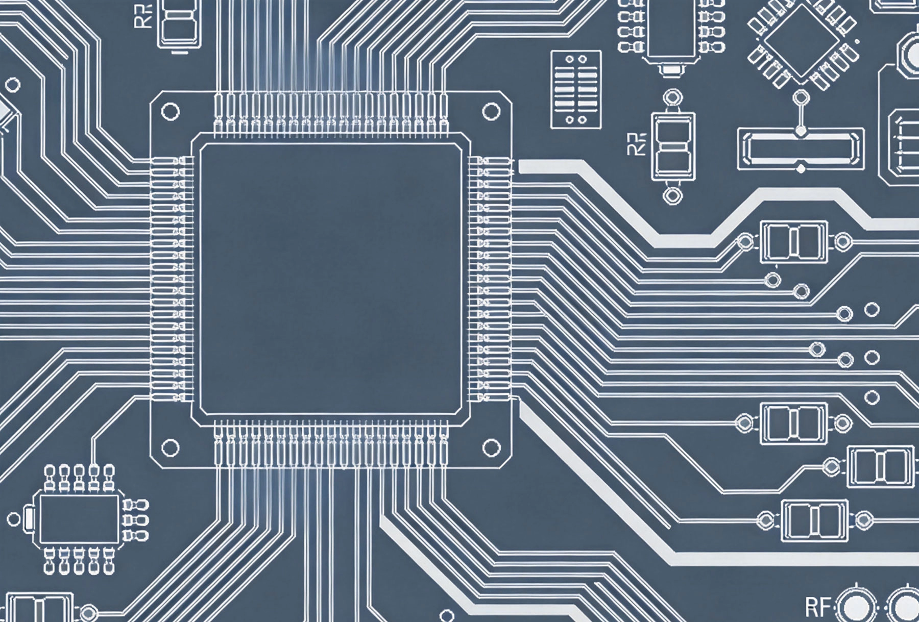
Before diving into prototype considerations, let's establish what impedance control means:
Characteristic impedance is the ratio of voltage to current for a propagating signal on a Transmission Line. For PCBs, this depends on:- Trace geometry (width, thickness)- Dielectric Constant of the substrate material- Dielectric thickness between trace and reference plane- Distance to neighboring traces and planes
Common impedance targets include:- 50Ω: Single-ended signals (Microstrip or stripline)- 100Ω differential: Differential pairs (LVDS, USB, Ethernet)- 90Ω differential: SATA, PCIe- 75Ω: Video and some RF applications
When signal traces have consistent characteristic Impedance Matching the source and load, signals propagate cleanly with minimal reflections. When impedance mismatches occur:- Signal energy reflects at impedance discontinuities- Reflected signals interfere with forward-traveling signals- Signal waveforms distort, causing timing errors- Eye diagrams close, increasing bit error rates
At high frequencies, even small impedance mismatches (5-10%) cause significant signal degradation.
What qualifies as "high-frequency" varies by application:
Here's the critical insight: a 100 MHz signal with a 1ns rise time contains frequency components up to 350 MHz (using the 0.35/tr rule of thumb). This means impedance control becomes important at clock frequencies lower than you might expect.
Engineers skip impedance control in prototypes for understandable reasons:
Logic: We're just proving the concept works; we'll fix details later. Reality: If Signal Integrity problems exist, they prevent proof of concept. Your prototype fails not because the concept is flawed, but because implementation details matter.
Logic: Controlled Impedance adds cost; let's wait for production. Reality: Uncontrolled impedance in prototypes costs more in the long run through redesigns, additional prototype cycles, and delayed product launches.
Logic: We need prototypes fast; controlled impedance takes time. Reality: Faster, cheaper prototypes without impedance control create problems that consume more time than saved.
Logic: Our prototype works fine; impedance control isn't needed. Reality: Bench tests don't reveal marginal signal integrity. Problems surface under:- Longer trace lengths in production- Different component placements- Manufacturing variations- Field conditions
Impedance mismatches in prototypes cause specific, measurable problems:
Impedance discontinuities cause signal reflections:- Reflection coefficient: Γ = (Z₂ - Z₁) / (Z₂ + Z₁)- 10% impedance mismatch: Creates 5% reflection- 25% impedance mismatch: Creates 11% reflection- These reflections: Add noise, distort waveforms, and close eye diagrams
Reflected signals cause timing problems:- Signal propagation delay: Affected by impedance variations- Setup and hold violations: Reflections cause edge jitter- Timing margin reduction: Marginal timing becomes problematic- Intermittent failures: Timing errors cause unpredictable behavior
Signal reflections reduce noise margin:- Signal-to-noise ratio degradation: Reflected signals add noise- Edge rate degradation: Reflections slow rise/fall times- Increased bit error rate: Noise and timing errors combine- Reduced distance: Signals can't travel as far reliably
Impedance mismatches create Emi problems:- Radiated emissions: Impedance discontinuities radiate energy- Emc testing failures: Designs fail regulatory testing- Interference with other circuits: Poor signal integrity causes crosstalk- Receiver sensitivity reduction: Emi makes circuits more susceptible
The true cost of skipping impedance control manifests in several ways:
Uncontrolled impedance creates false confidence:- Prototype passes functional tests on the bench- Design team assumes concept is proven- Production boards fail subtle tests- Team realizes foundation was flawed all along
Signal integrity problems trigger redesigns:- Original prototype: 4 weeks, $2,000- Redesign: additional 4 weeks, $2,000- Second prototype: 2 weeks, $1,000- Total waste: 6 weeks, $3,000 (minimum)
With controlled impedance from the start:- Prototype: 4.5 weeks, $2,200- Production transition: direct- Total: 4.5 weeks, $2,200
Even if prototypes work, production reveals issues:- Manufacturing variations affect impedance- Longer production boards have different characteristics- Component Placement variations create mismatches- Production yield drops due to marginal designs
Marginal designs fail in the field:- Intermittent errors appear only in field conditions- Temperature variations exacerbate problems- Customer dissatisfaction increases- Warranty costs escalate
Not all designs require impedance control. Here's when it becomes critical:
The critical length formula: L_critical = (rise_time) × (velocity_factor) Example: For a 2ns rise time signal traveling at 150 ps/inch:- Critical length = 2ns / 150ps/inch = 13.3 inches Traces longer than 1/4 to 1/3 of critical length require impedance control.
Impedance control in prototypes doesn't have to be expensive or time-consuming:
Let's examine the actual costs of impedance control:
Scenario A: Skip impedance control - Prototype cost: $250- Redesign cost: $3,000 (additional prototypes + engineering time)- Production risk: Marginal design- Total: $3,250+
Scenario B: Include impedance control - Prototype cost: $300- Redesign cost: $0 (works first time)- Production risk: Proven design- Total: $300
Even for a single prototype, the ROI is clear. For production, the advantage becomes overwhelming.
Verification confirms your design meets requirements:
Problem: Not specifying dielectric thickness, copper weight, or material Dk. Solution: Provide complete stack-up specification including all material properties.
Problem: Routing controlled impedance over plane splits or gaps. Solution: Ensure continuous reference planes under all controlled impedance signals.
Problem: Excessive vias causing impedance variations. Solution: Minimize vias, use back-drilling for high-frequency signals, or use via-in-pad techniques.
Problem: Dk variations across the board or between lots. Solution: Specify materials with tight Dk tolerances, work with manufacturers who control materials.
Problem: Assuming design meets impedance without verification. Solution: Always measure impedance on prototypes, especially first article.
Successful impedance control in prototypes enables smooth production transition:
For demanding high-frequency applications:
Follow established standards for impedance control:
Impedance control in High-frequency Pcb prototypes isn't optional—it's essential. The apparent cost savings from skipping impedance control are illusions that hide expensive downstream costs: redesign cycles, production failures, and field returns.
The investment in impedance control during prototyping pays dividends in:- Faster development cycles (no redesigns)- Reduced total project cost- Higher confidence in production success- Better product reliability- Improved time-to-market
Modern high-frequency designs, even in prototype phases, require transmission line thinking. Treat impedance control as a fundamental design parameter, not a production detail. The discipline of proper impedance control from the first prototype creates designs that work reliably from bench through production to field deployment.
Need help implementing impedance control in your High-frequency Pcb prototypes? Work with PCB manufacturers who understand high-speed design requirements. Their expertise in material selection, stack-up design, and impedance verification ensures your prototypes provide reliable, transferable results to production.
Common Pitfalls to Avoid During Your High Frequency PCB Prototype PhaseJune/18/2026
Turnkey High Frequency PCB Prototype Services: Streamlining Your Development CycleAugust/06/2026
How to Choose the Best High Frequency PCB Prototype Supplier for StartupsSeptember/10/2026

The Cost of High Frequency PCB Prototyping: What Influences the Price?July/26/2026
The Importance of Thermal Management in High Frequency PCB AssemblyJuly/27/2026
Testing and Validation: Ensuring Your High Frequency PCB Prototype Meets SpecsAugust/15/2026
High Frequency PCB Prototype vs. Mass Production: Key Differences in FabricationJune/05/2026
The Benefits of Rapid High Frequency PCB PrototypingMay/29/2026