Open Nav

The Artificial Intelligence revolution has created unprecedented demand for computing infrastructure capable of handling massive parallel processing workloads. Training large language models and running inference at scale requires server hardware that pushes the boundaries of electrical engineering. At the heart of these AI servers lie advanced high frequency PCBs that enable the signal speeds, power delivery, and thermal management that modern AI workloads demand. Without these specialized circuit boards, the current generation of AI accelerators would simply not function. Understanding how high frequency PCB technology enables AI computing helps engineers appreciate the critical role that materials science and manufacturing expertise play in the AI revolution.

AI workloads fundamentally differ from traditional computing tasks in their demand for parallel processing and memory bandwidth. Training neural networks involves enormous matrix multiplications that benefit from thousands of processing cores working simultaneously. This parallel processing architecture requires interconnects capable of moving data between chips at rates exceeding hundreds of gigabytes per second. Traditional server architectures built for serial processing cannot meet these requirements without fundamental changes to their core electronics.
The bandwidth requirements for AI accelerators have grown exponentially. A single GPU in an AI training cluster might require 900 watts of power and generate heat that must be removed efficiently. The printed circuit boards connecting these devices must handle not just high-speed signals but also massive current distribution without introducing voltage drops that would compromise computing accuracy. Every millivolt of noise in a power distribution network can introduce errors in the analog circuits that convert digital signals to the physical world.
Thermal management has become one of the primary constraints limiting AI computing performance. As transistor densities increase and switching speeds accelerate, power density in AI accelerators approaches limits that challenge conventional cooling approaches. The PCB itself becomes part of the thermal solution, with specialized materials and designs that conduct heat away from hot components while maintaining the electrical performance required for high-speed operation.
Signal Loss in PCBs increases with frequency, making material selection critical for AI server applications. Standard FR4 materials introduce significant attenuation at the multi-gigahertz frequencies used in modern AI interconnects. Advanced materials like Rogers RO4000 series, Panasonic Megtron 6, and Isola ITERGY Frequency feature loss tangents below 0.002 at 10 GHz, compared to 0.02 for standard FR4. This tenfold improvement in loss characteristics enables longer trace runs without signal degradation and reduces the power required to drive signals across the board.
The Dielectric Constant stability of advanced materials across temperature and frequency ranges also matters for AI applications. Rogers materials maintain consistent dielectric properties from DC through microwave frequencies, enabling predictable Impedance Control throughout the signal bandwidth. This consistency allows designers to create Transmission Lines that perform reliably across the entire operating range of AI accelerators, which may generate significant self-heating during operation.
Japanese material manufacturers have developed ultra-low-loss materials specifically optimized for AI server applications. Panasonic Megtron 6 offers a loss tangent of 0.001 at 10 GHz while maintaining processability similar to standard materials. This combination of electrical performance and manufacturing compatibility has made Megtron 6 the preferred choice for AI accelerator modules where Signal Integrity and yield both matter.
Shengyi S1000 series materials provide cost-competitive alternatives with loss tangents around 0.002. While slightly higher than Megtron 6, these materials enable AI server manufacturing at scale where material costs significantly impact system pricing. The performance gap between premium and standard materials continues to narrow as manufacturers develop improved formulations.
AI servers rely on serial links operating at 112 gigabits per second per lane to connect accelerators within a system. These incredibly fast signals require Transmission Line designs that maintain Signal Integrity over the lengths needed for board-level interconnects. At 112 Gbps, a bit period is less than 9 picoseconds, meaning any discontinuity shorter than a millimeter can create measurable reflection that degrades eye opening.
The transition to 112G SerDes has driven adoption of advanced PCB technologies previously reserved for telecommunications and aerospace. Differential pairs with precisely Controlled Impedance, tight spacing tolerances, and sophisticated via designs all become essential when operating at these speeds. AI server manufacturers now specify impedance tolerances of plus or minus 7 percent or tighter, compared to plus or minus 10 percent considered adequate for previous-generation servers.
Eye diagrams at 112 Gbps show the combined effect of jitter, noise, and intersymbol interference. Opening the eye sufficiently for reliable detection requires minimizing every source of signal degradation. PCB designers use electromagnetic simulation to optimize trace geometry, control via stubs through back-drilling, and balance differential pairs to within 0.1 millimeters over the full trace length.
AI servers use PCIe and Compute Express Link standards to connect accelerators, storage, and memory. PCIe 6.0 operates at 64 GT/s per lane, requiring the same extreme signal integrity as 112G SerDes. CXL adds cache coherency features that introduce additional protocol complexity while maintaining the same physical layer requirements.
The PCB interconnect budget for these standards allocates margin for connector losses, routing discontinuities, and material dispersion. Designers must account for crosstalk between adjacent differential pairs, which becomes more significant as trace spacing decreases. Shielding techniques including ground trace routing between pairs and specialized connector designs help maintain signal quality across the full channel.
Modern AI accelerators like NVIDIA H100 GPUs consume up to 700 watts during training workloads. Delivering this power through a PCB while maintaining voltage regulation within tight tolerances requires thick copper planes, distributed voltage regulation modules, and careful thermal management. The PCB becomes a critical component of the power delivery network, not just a substrate for signal routing.
Voltage regulator modules positioned close to the accelerator chip reduce the distance that high current must travel through the PCB. This distributed architecture minimizes resistive losses and voltage drop, but requires the PCB to handle current densities exceeding 100 amps per square millimeter in the heaviest current paths. Heavy copper constructions with 3-ounce or 4-ounce copper planes provide the current capacity needed while maintaining planarity for reliable component mounting.
AI accelerators switching at gigahertz frequencies generate noise that can corrupt adjacent signal traces if not properly suppressed. Decoupling capacitors placed directly on the PCB near power pins provide local energy storage that filters high-frequency noise. However, the inductance of capacitor packages and PCB routing limits effectiveness above certain frequencies.
Embedded capacitance technology addresses high-frequency decoupling requirements by placing thin high-capacitance dielectrics between power and ground planes. These embedded capacitors provide extremely low series inductance, filtering noise at frequencies where discrete capacitors lose effectiveness. Some AI server boards use multiple layers of embedded capacitance to address different frequency ranges throughout the power distribution network.
The resistance of PCB copper traces generates heat when carrying the high currents required by AI accelerators. This self-heating raises temperature, which increases resistance in a positive feedback loop that can lead to thermal runaway if not properly managed. PCB designers must calculate temperature rise under maximum current conditions and ensure adequate copper weight and trace width to keep temperatures within acceptable limits.
Thermal vias connecting power planes to external heatsinks or liquid cooling structures provide heat spreading and removal. These thermal pathways must not compromise the electrical performance of signal layers, requiring careful design to isolate thermal and electrical functions. Some advanced AI server boards integrate active cooling channels directly into the PCB structure, blurring the line between electronics and thermal management hardware.
Achieving the trace geometries required for 112 Gbps signaling demands fabrication capabilities that push the limits of standard Pcb Manufacturing. Line widths below 3 mils with tolerances of plus or minus 0.3 mils require advanced imaging and etching processes. Panel sizes of 24 by 18 inches or larger must maintain this precision across the entire area, requiring sophisticated process controls and equipment calibration.
Yield at these tolerances depends critically on material consistency and process stability. Even small variations in copper grain structure or dielectric composition can shift impedance enough to cause failures. The most advanced AI server manufacturers have developed proprietary processes that achieve yields sufficient for commercial production at these dimensions.
Through-hole vias connecting power and ground planes must carry currents exceeding 100 amps in some AI server applications. These high-current vias require heavy plating that fills the barrel completely without voids. The aspect ratios involved, sometimes exceeding 10:1 for thick boards, challenge traditional plating chemistry and require specialized additive packages to achieve uniform coverage.
Blind and buried vias in multilayer AI server boards require precise sequential lamination that maintains registration between layers to within 0.5 mils. The layer count for AI accelerator modules may reach 20 or more, creating complex stackups where each layer must be fabricated and integrated without introducing defects that would compromise yield.
Testing AI server PCBs requires measurement capabilities matched to the performance requirements. Time domain reflectometry at 20 GHz bandwidth can resolve impedance variations along traces, identifying discontinuities that would cause failures at operating speeds. Automated optical inspection with sub-micron resolution detects surface defects that could lead to reliability problems.
Electrical testing must verify not just basic connectivity but signal integrity performance. Some manufacturers test sample boards with eye diagram measurements at full data rates, accepting statistical sampling rather than 100 percent testing due to the time required. X-ray Inspection verifies internal structures including blind via quality and plating uniformity for critical nets.
The next generation of AI interconnects will operate at 224 Gbps per lane, doubling the current data rate while maintaining the same form factor. This doubling will require even lower loss materials, finer line geometries, and more sophisticated equalization circuits to open eye diagrams sufficiently. PCB material manufacturers are developing next-generation laminates with loss tangents below 0.0005 to support these requirements.
Optical interconnects will increasingly supplement or replace electrical links for the longest connections. PCB manufacturers are developing hybrid structures that integrate optical waveguides alongside traditional copper traces. These photonic PCBs could enable AI servers to scale beyond the limits imposed by electrical interconnect density and power consumption.
The shift toward chiplet-based AI accelerators changes PCB requirements significantly. Instead of routing signals between large monolithic chips, AI systems will connect multiple smaller chiplets at close proximity. This change drives demand for very high density substrates that may use chip-on-wafer or panel-level packaging technologies rather than traditional PCB Fabrication.
Organic interposer technology bridges the gap between standard PCBs and silicon interposers. These substrates use PCB-like materials and processes but achieve densities approaching silicon. Some AI accelerator manufacturers have qualified organic interposers as lower-cost alternatives to silicon for medium-density chiplet integration.
What frequency ranges do AI server PCBs typically operate at?
AI server interconnects operate at frequencies from DC for power distribution through tens of gigahertz for high-speed serial links. The primary signal content sits between 1 GHz and 30 GHz, corresponding to the fundamental frequencies of 56 Gbps and 112 Gbps data rates. Power distribution networks carry energy from DC to megahertz ranges, while clock distribution and control signals occupy the megahertz to gigahertz spectrum.
Why do AI servers require more advanced Pcb Materials than standard servers?
The combination of extreme bandwidth requirements, tight signal integrity budgets, and high power density creates challenges that standard materials cannot address. Loss characteristics that are acceptable for 10 Gbps interconnects introduce unacceptable attenuation at 112 Gbps. Thermal management requirements that are manageable at 200 watts become critical at 700 watts. The multiplicative effect of these requirements drives adoption of advanced materials throughout AI server designs.
How do PCB manufacturers achieve the tolerances required for AI server applications?
Advanced manufacturers use statistical process control, sophisticated imaging systems, and proprietary process recipes to achieve the required tolerances. Optical proximity correction in imaging, precise temperature and humidity control in processing, and automated in-process metrology all contribute to achieving tight tolerances at scale. The investment in process capability represents a significant competitive advantage for manufacturers serving the AI market.
What role does simulation play in AI server PCB design?
Simulation is essential for achieving signal integrity at AI server data rates. Electromagnetic simulators predict crosstalk, impedance, and radiation characteristics. Thermal simulators identify hotspots and optimize heat spreading. Power integrity tools analyze voltage drop and switching noise. These simulations reduce the number of design iterations needed to achieve performance targets, which is critical given the compressed development cycles typical for AI hardware.
How is AI server Pcb Reliability verified?
AI server PCBs undergo accelerated life testing including thermal cycling, temperature humidity bias, and vibration testing. These tests verify that designs will survive the operating conditions expected in data center environments. High-temperature operating life testing addresses the elevated temperatures that AI accelerators generate during extended training workloads. Failure analysis on any test failures guides design improvements for subsequent iterations.
high frequency PCB technology forms the invisible foundation of the AI revolution. Without advanced materials, precise manufacturing, and sophisticated design techniques, the AI accelerators driving machine learning breakthroughs would remain impractical. The requirements of AI computing have pushed PCB technology to its limits and beyond, driving innovation in materials science, fabrication processes, and design methodology.
The collaboration between AI accelerator designers and PCB specialists continues to evolve as both fields advance. Materials manufacturers develop new laminates optimized for AI requirements. PCB fabricators invest in capabilities that serve the most demanding applications. Designers develop simulation and design techniques that extract maximum performance from available technology. This ecosystem of continuous improvement enables the exponential growth in AI computing capability that the market demands.
Understanding the role of high frequency PCBs in AI servers provides perspective on the breadth of engineering advancement required to achieve modern computing capabilities. While much attention focuses on chip architectures and algorithms, the electronic packaging that connects chips at high speed represents equally impressive technical achievement. As AI demands continue growing, PCB technology will advance in step, enabling the next generation of intelligent computing infrastructure.
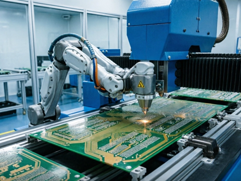
From Prototype to Mass Production: Scaling with a Reliable High Frequency PCB ManufacturerJuly/13/2026
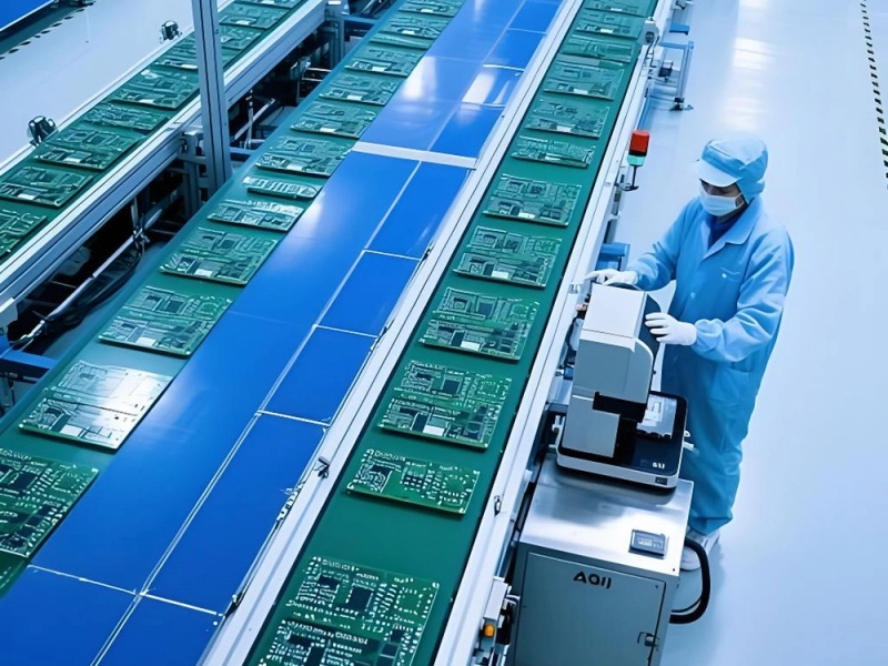
7 Key Factors to Consider When Choosing a High Frequency PCB ManufacturerMay/29/2026
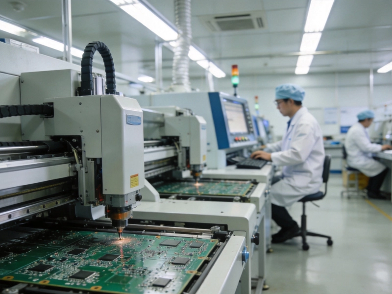
Top 5 Questions to Ask Your High Frequency PCB Manufacturer Before Placing an OrderAugust/14/2026
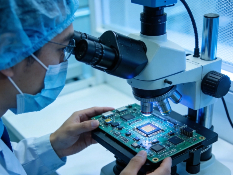
How to Vet a High Frequency PCB Manufacturer for 5G and Millimeter Wave ProjectsJuly/25/2026
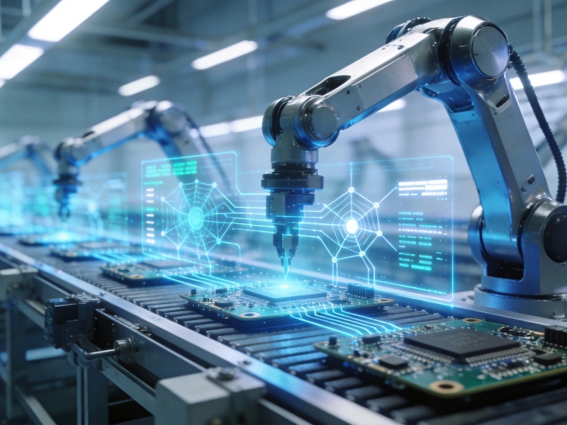
The Role of AI in Modern High Frequency PCB Manufacturing: Precision and EfficiencyJune/30/2026
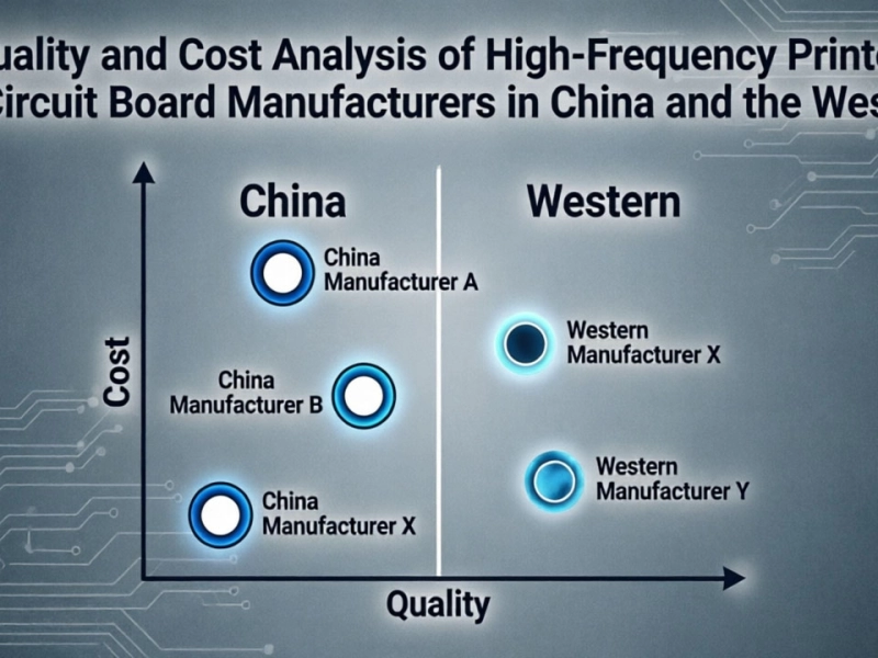
Quality and Cost Analysis of High-Frequency Printed Circuit Board Manufacturers in China and the WestJune/04/2026
Case Study: How the Right High Frequency PCB Manufacturer Solved a Critical EMI IssueSeptember/09/2026
Inside the Factory: What to Look for in a High Frequency PCB Manufacturer's FacilityAugust/03/2026