Open Nav

When a leading RF communication equipment manufacturer faced unexpected electromagnetic interference issues in their latest 5g Base Station design, their existing PCB supplier could not identify the root cause. Despite meeting all specified tolerances, the boards radiated emissions that exceeded regulatory limits and caused adjacent channel interference in field deployments. This case study details how engaging a specialized high frequency PCB manufacturer transformed their product from a compliance failure to a market success.
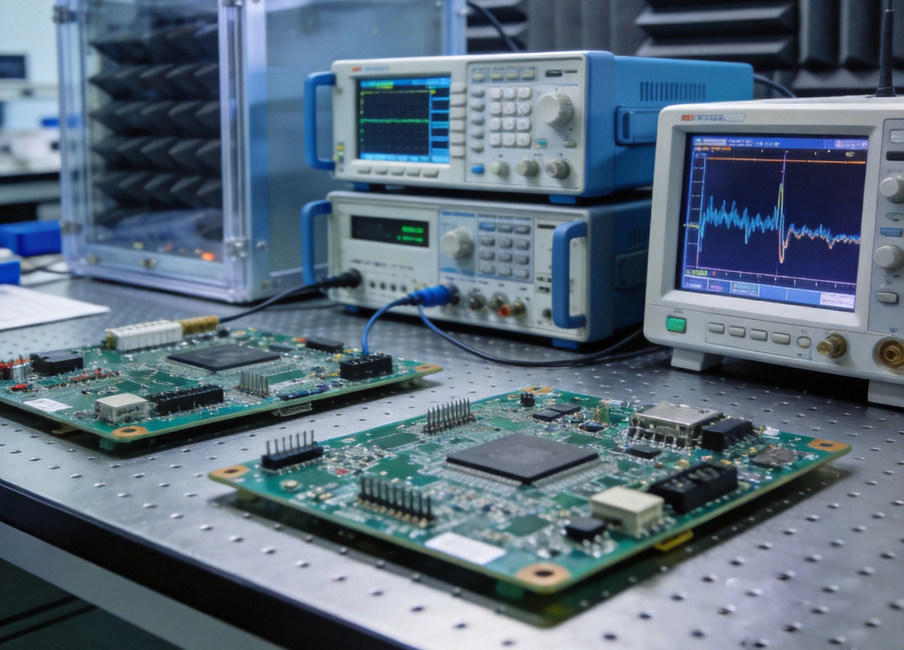
The manufacturer had developed a new multi-layer PCB design for a 28GHz 5G remote radio unit. The board featured high-speed data converters, RF front-end components, and power regulation circuits all on a 16-layer stackup measuring 300mm by 200mm. Initial prototypes passed laboratory testing but failed consistently during pre-certification Emi testing at an accredited laboratory.
The specific failure modes included:
Their original supplier, while technically competent for standard digital boards, lacked the specialized expertise to diagnose high frequency electromagnetic behavior. After three months of unsuccessful attempts to resolve the issue through layout modifications, the manufacturer sought alternative expertise.
The specialized high frequency PCB manufacturer began with a comprehensive assessment of the existing design and manufacturing approach.
Initial review identified several areas of concern:
Beyond design, manufacturing process evaluation revealed additional issues:
Through systematic analysis using Electromagnetic Simulation and measurement, the team identified the primary root causes of the Emi failures.
The most significant problem stemmed from impedance discontinuities throughout the signal path. Standard IPC impedance tolerances of +/- 10% became unacceptable at 28GHz, where even small discontinuities create significant reflection and radiation.
Time-domain reflectometry measurements revealed impedance variations of 15-20% at critical nodes, far exceeding the 5% tolerance required for Stable Rf Performance.
Ground Plane segmentation, while common in digital designs to isolate noise sources, created serious problems at RF frequencies. Current return paths had to route around gaps in the ground structure, creating effective antenna structures that radiated efficiently.
Standard Fr-4 material exhibits significant dielectric loss at 28GHz, with Dissipation Factor (Df) around 0.02. At the operating frequency, this loss contributed to signal degradation and created thermal hot spots in high-power sections. The material also demonstrated inconsistent Dk values across the panel, affecting phase response.
Based on the root cause analysis, the manufacturer implemented a comprehensive solution addressing both design and manufacturing factors.
The first change involved transitioning from standard FR-4 to a specialized high-frequency laminate:
The board stackup underwent fundamental redesign:
Signal routing received extensive revision:
Manufacturing process modifications addressed process-related variations:
The modified design underwent extensive testing to verify EMI performance improvement.
Pre-certification testing demonstrated dramatic improvement:
Beyond compliance, field performance validated the approach:
Process improvements yielded manufacturing benefits:
This case study provides valuable insights for engineers and procurement teams working with high-frequency electronics.
Key takeaways for PCB design include:
Supplier selection considerations include:
Effective high-frequency manufacturing requires:
While specialized high-frequency manufacturing involves higher unit costs, the total value proposition proved compelling.
Comparing the original and specialized approaches:
Beyond immediate problem resolution:
The diagnosis and validation employed specific measurement techniques.
Impedance measurements used:
Emissions testing followed established procedures:
Material characterization included:
This case study demonstrates that EMI issues in High-frequency Pcb assemblies often require specialized expertise beyond standard manufacturing capability. The combination of appropriate material selection, design optimization for RF performance, and manufacturing process controls specifically for high-frequency applications enabled a successful resolution where conventional approaches had failed.
For engineers developing high-frequency electronics, engaging specialized manufacturers early in the design process can prevent costly problems later. The additional investment in expertise and materials yields returns through improved first-pass success, reduced field failures, and faster time-to-market for reliable products.
The manufacturer involved in this case now maintains a long-term partnership with the High-frequency Pcb specialist, leveraging their expertise across multiple product generations. This collaborative relationship has prevented EMI issues in subsequent designs while continuously improving manufacturing processes and design guidelines.
From Prototype to Mass Production: Scaling with a Reliable High Frequency PCB ManufacturerJuly/13/2026
Why Certifications Matter: IATF16949 and ISO Standards for Your High Frequency PCB ManufacturerJune/17/2026

How to Vet a High Frequency PCB Manufacturer for 5G and Millimeter Wave ProjectsJuly/25/2026
7 Key Factors to Consider When Choosing a High Frequency PCB ManufacturerMay/29/2026
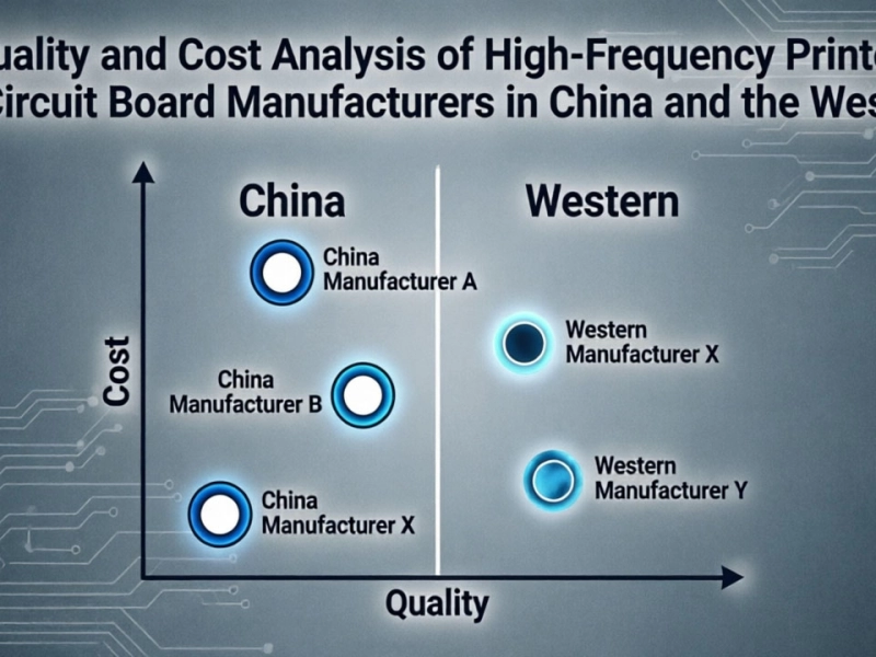
Quality and Cost Analysis of High-Frequency Printed Circuit Board Manufacturers in China and the WestJune/04/2026
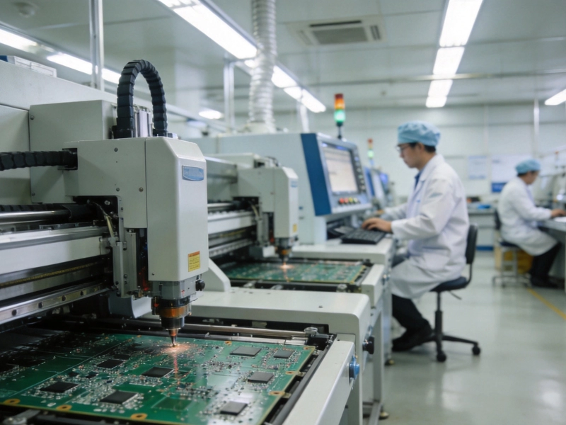
Top 5 Questions to Ask Your High Frequency PCB Manufacturer Before Placing an OrderAugust/14/2026
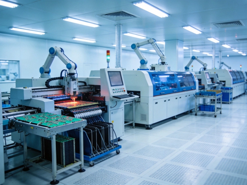
Inside the Factory: What to Look for in a High Frequency PCB Manufacturer's FacilityAugust/03/2026

How High Frequency PCB Applications are Powering the AI Server RevolutionAugust/03/2026