Open Nav

As the demand for faster data transmission, higher frequency wireless communication, and more sophisticated electronic systems continues to grow, high frequency PCBs have become one of the most technically demanding segments of the electronics manufacturing industry. From 5G base stations and radar systems to Automotive Radar, Satellite Communications, and high-speed data centers, these applications operate at frequencies ranging from a few gigahertz to over 100 GHz—pushing the limits of what traditional Pcb Manufacturing processes can reliably achieve.
At high frequencies, even the smallest deviations from design specifications can have outsized effects on circuit performance. A trace width variation that would be completely insignificant at 100 MHz can cause catastrophic Signal Integrity problems at 28 GHz or 77 GHz. This is why fabrication tolerances for high frequency PCBs are tighter and more critical than ever before, and why choosing a manufacturer with the precision, process control, and expertise to meet those tolerances is one of the most important decisions in any high frequency PCB project.
This article explores why precision matters so much in high frequency PCB Fabrication, the specific tolerances that are most critical, how leading manufacturers achieve these tolerances, and what engineers need to know when specifying and designing for high frequency applications.
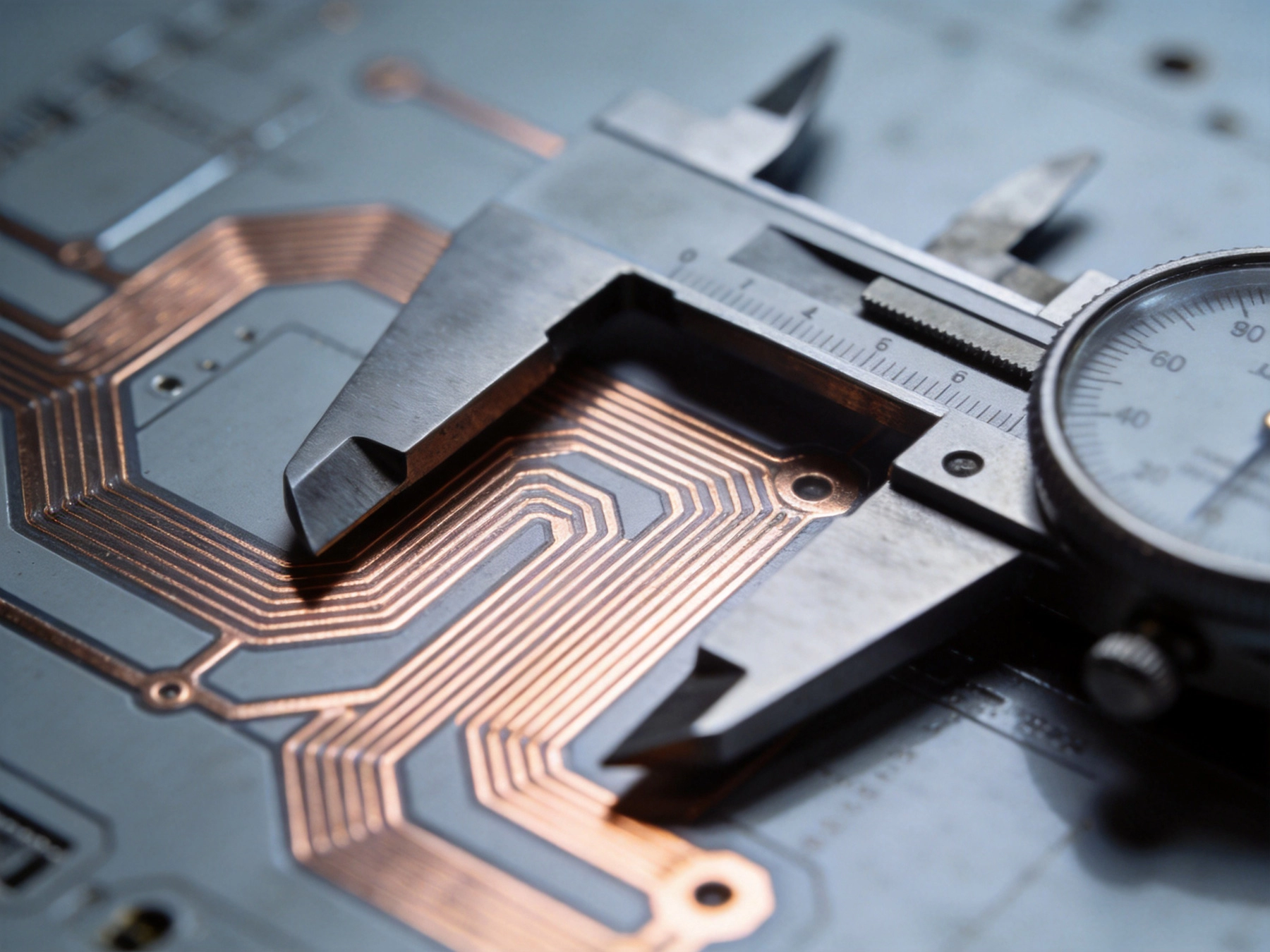
To understand why fabrication tolerances matter so much for high frequency PCBs, it helps to understand some basic principles of high frequency signal behavior. At low frequencies, the electrical characteristics of a PCB trace are relatively forgiving. A slightly wider trace or a marginally different dielectric thickness has negligible effect on circuit performance. The signals behave essentially as they do in DC circuits—current flows through conductors, and voltage drops predictably along traces.
At high frequencies, everything changes. Signals no longer behave as simple voltages and currents; instead, they behave as electromagnetic waves traveling along Transmission Lines. The physical dimensions of the trace, the dielectric properties of the substrate, and the geometry of the PCB all become critical parameters that determine how these electromagnetic waves propagate. Small variations in any of these parameters cause significant changes in key electrical characteristics like impedance, Insertion Loss, and phase velocity.
The critical factor is wavelength. At 1 GHz, the wavelength of a signal in a typical PCB dielectric is about 15 centimeters. At 28 GHz (a common 5G frequency), the wavelength shrinks to about 5 millimeters. At 77 GHz (Automotive Radar), the wavelength is only about 2 millimeters. When trace dimensions approach a significant fraction of the signal wavelength—even as little as 1/10th to 1/20th—the Transmission Line effects become dominant, and the circuit behaves as a distributed parameter system rather than a lumped circuit.
In a distributed system, a trace that is even 0.1mm longer or shorter than intended represents a measurable electrical length difference. A variation in trace width that changes the impedance by even 1 ohm can cause significant reflection of the signal. These effects accumulate along the length of the trace, making the overall circuit performance highly sensitive to cumulative manufacturing variations.
The most critical electrical parameter in high frequency PCBs is Characteristic Impedance. For a Microstrip or stripline Transmission Line, the impedance is determined by the trace width, trace thickness, dielectric thickness, and the Dielectric Constant of the substrate material. The impedance formula for a Microstrip is:
Z0 = (87 / sqrt(er + 1.41)) * ln(5.98H / (0.8W + T))
where Z0 is the Characteristic Impedance, er is the relative Dielectric Constant, H is the dielectric height, W is the trace width, and T is the trace thickness. While the full calculation is more complex in practice, this simplified formula illustrates the point: impedance is a function of multiple variables, each of which has a tolerance associated with it.
For a typical 50-ohm microstrip, the manufacturing tolerances must be controlled to keep the impedance within ±5%, ±3%, or even ±1% depending on the application. At 28 GHz, a 5% impedance tolerance might be acceptable for some applications, but for automotive radar or precision measurement equipment, tolerances of ±2% or tighter are often required. Achieving these tolerances requires extremely tight control over every parameter in the impedance equation.
The dielectric constant (Dk or er) of the substrate material is one of the most critical and least controllable parameters in high frequency PCB design. Dielectric constant is not a fixed value—it varies with frequency, temperature, and humidity. Even more challenging, dielectric constant varies from batch to batch and even within a single panel of material due to variations in resin content, filler distribution, and cure conditions.
A typical Fr-4 material might have a dielectric constant of 4.4 at 1 MHz that decreases to 4.1 at 1 GHz—a 7% change with frequency alone. High-performance High Frequency Materials like Rogers Ro4003c have much more stable dielectric constants (3.38 ± 0.05 at 10 GHz), but even these small variations can be significant at very high frequencies. Manufacturers must carefully characterize their materials and account for these variations in their impedance calculations.
Trace width is one of the most directly controllable parameters in Pcb Manufacturing, and also one of the most critical for high frequency performance. For a 50-ohm microstrip on a typical substrate, a 10% increase in trace width might reduce impedance by 3-5 ohms—enough to cause significant reflection at high frequencies.
Standard PCB Fabrication tolerances for trace width are typically ±20% for simple boards, but this is completely unacceptable for high frequency applications. Leading high frequency pcb manufacturers achieve trace width tolerances of ±10% to ±15% as standard, with premium manufacturers achieving ±5% or better for critical designs. Some ultra-precision manufacturers can achieve ±2% trace width tolerance for the finest features, though this requires specialized processes and extensive quality control.
Trace spacing tolerances are equally important, especially for coupled differential pairs and tight multi-lane bus designs. Variations in spacing affect coupling coefficients and can cause imbalance in differential pairs, leading to common-mode noise and Emi problems. Differential pair spacing tolerances are typically specified in absolute terms (e.g., ±0.02mm) rather than percentage terms, since percentage tolerances become meaningless at very tight spacings.
The dielectric thickness between the signal trace and the Ground Plane directly affects impedance, making thickness control critical for high frequency boards. Standard PCB laminates have thickness tolerances of ±10% to ±15%, but high frequency boards typically require ±5% or better, with some applications demanding ±2% or tighter.
Thickness control is especially challenging for multi-layer boards, where the overall board thickness and the thickness of individual dielectric layers must both be controlled. Layer thickness variations arise from prepreg flow during lamination, press pressure variations, and material property variations. Achieving tight dielectric thickness tolerances requires careful material selection, controlled lamination processes, and in-process measurement and correction.
Vias in high frequency circuits must be treated as transmission line discontinuities, and their dimensions and placement must be controlled with the same precision as traces. Via stub length, pad diameter, anti-pad size, and via-to-trace spacing all affect high frequency performance. A via with excessive stub length can act as a resonant stub at certain frequencies, causing deep nulls in the frequency response.
Via placement tolerances affect trace-to-via transitions, which are critical for Impedance Matching. Via position errors as small as 0.05mm can cause impedance mismatches at very high frequencies. For applications like 5G phased array antennas where hundreds of identical element circuits must match precisely, via placement errors can cause systematic beam-pointing errors that cannot be corrected in firmware.
As discussed earlier, dielectric constant variation is one of the most challenging tolerances in high frequency pcb manufacturing. Material datasheets typically specify Dk as a nominal value with a tolerance range, but the actual Dk can vary with frequency, temperature, and humidity in ways not fully captured by the datasheet specification.
High Frequency Pcb manufacturers address Dk variation through several strategies: using premium-grade high frequency laminates with tighter Dk tolerances, performing incoming material testing to measure actual Dk values, mapping Dk variation across panels and accounting for it in impedance calculations, and using impedance test coupons placed adjacent to production panels to validate actual impedance on each production run.
Dimensional tolerances affect the overall size and shape of the PCB, which matters for mechanical fit in the end application and for panel utilization during manufacturing. But for high frequency circuits, registration tolerances—the accuracy with which layers are aligned relative to each other—can be even more critical.
Layer-to-layer registration errors cause misalignments between signal traces and ground planes, between pads and vias, and between layers in multi-layer constructions. At high frequencies, these misalignments cause impedance variations, mode conversion (from differential to common mode), and increased radiation. Registration tolerances of ±0.05mm are typical for standard PCBs, but high frequency boards may require ±0.025mm or tighter.
The surface finish on a High Frequency Pcb affects the current distribution within the conductor and the effective conductor roughness, both of which influence Insertion Loss at high frequencies. Different surface finishes add different amounts of metal to the trace, which affects the effective trace width and impedance. The finish process itself (immersion silver, ENIG, HASL) can also affect the surface roughness of the underlying copper.
For high frequency applications, ENIG (electroless nickel immersion gold) is often preferred because the thin, uniform gold layer has minimal impact on impedance and provides a consistently smooth surface. However, the nickel layer beneath must be controlled for thickness, as excessive nickel can increase losses. HASL (hot air solder leveling) is generally avoided for high frequency applications because the uneven application and relatively thick layer can cause significant impedance variation.
Meeting the tight tolerances required for high frequency PCBs requires a combination of premium materials, advanced equipment, rigorous process control, and extensive testing. Leading high frequency PCB manufacturers employ several key strategies:
High frequency PCB manufacturers start with premium-grade high frequency laminates from reputable suppliers like Rogers, Isola, Panasonic, or Taconic. These materials are manufactured to tighter specifications than standard Fr-4 and have more consistent dielectric properties. However, even premium materials require verification. Leading manufacturers test incoming materials for actual Dk and Df (Dissipation Factor) using techniques like the split post dielectric resonator (SPDR) method or differential phase length method, and maintain databases of material properties by lot number for traceability.
Trace width control begins with the imaging process. Direct laser imaging (DLI) systems achieve much finer resolution and better critical dimension control than traditional film-based imaging, which introduces additional variation from film dimensional instability. Advanced manufacturers use LDI systems with laser spot sizes of 20µm or smaller, achieving trace width control of ±5% or better on the finest features.
Etching process control is equally important. Over-etching or under-etching directly affects trace width. Leading manufacturers use statistical process control (SPC) to monitor and adjust etching parameters in real time, maintaining tight control over the etch process. Some manufacturers use plasma etching or other advanced techniques that offer better control than conventional chemical etching for fine-feature boards.
Lamination is one of the most critical and least controllable steps in multi-layer PCB manufacturing. Variations in pressure, temperature, and time during lamination affect dielectric thickness, layer registration, and material properties. High frequency manufacturers use advanced hydraulic or Vacuum Lamination presses with precise temperature and pressure control, often with multi-zone heating to ensure uniform heat distribution across the panel.
Some manufacturers use sequential lamination with careful intermediate testing between steps to catch and correct problems before they compound. Others use buildup processes that allow tighter control over individual layer thicknesses than traditional multi-layer lamination.
High frequency PCB manufacturers employ extensive in-process inspection and testing to verify that tolerances are being met during production. This includes:
Achieving tight tolerances is not a one-time achievement but an ongoing process of continuous improvement. Leading manufacturers use statistical process control (SPC) to monitor key process parameters, identify trends before they cause out-of-tolerance conditions, and drive continuous improvement in process capability. They track Cpk (process capability index) for critical parameters and set aggressive targets (Cpk > 1.33 or even 1.67 for the most critical parameters) to ensure that tolerances are maintained with substantial safety margin.
Even with the most precise manufacturing capabilities, designers can take steps to make their high frequency PCB designs more robust to manufacturing variations:
Specify tolerances that are achievable and necessary for your application, not tighter than you actually need. Tighter tolerances always cost more and may reduce yield, so balance precision requirements against cost and manufacturability. If your application can tolerate ±5% impedance variation, do not specify ±2% unless you have a specific reason to do so.
Trace width tolerances are typically specified as a percentage of the target width. A 0.2mm trace with ±5% tolerance has a possible variation of 0.01mm, while a 0.5mm trace with the same ±5% tolerance has a possible variation of 0.025mm. Using wider traces (where your layout allows) reduces the absolute variation and makes impedance easier to control. For high frequency applications, 50-ohm traces are often designed at 0.4-0.6mm rather than pushing for minimum width.
Design your circuits with margin that can absorb some manufacturing variation. For example, if your system requires 45-55 ohm impedance, design the nominal target at 50 ohms with enough margin that even worst-case manufacturing variation stays within your 45-55 ohm requirement. This approach reduces sensitivity to manufacturing variations and improves production yield.
Dielectric constant and trace dimensions both vary with temperature. Your design should account for these variations, especially if the board will operate over a wide temperature range. Similarly, dielectric constant varies with frequency, so ensure your impedance calculations are based on dielectric constant values at the actual operating frequency, not at lower frequencies.
Full ground planes adjacent to signal traces provide a consistent reference and reduce sensitivity to dielectric thickness variations. Via Stitching between ground planes at regular intervals reduces Ground Plane impedance and improves Signal Integrity, especially at very high frequencies. These design practices do not eliminate the need for tight manufacturing tolerances, but they reduce the sensitivity of circuit performance to those tolerances.
The consequences of failing to meet fabrication tolerances in high frequency PCBs range from minor performance degradation to complete system failure, depending on the application and the magnitude of the violation:
High Frequency Pcb Fabrication tolerances are more critical than ever before, driven by the demands of 5G communications, automotive radar, satellite systems, and other advanced applications that push frequencies and performance requirements to their limits. Understanding why these tolerances matter, which specific tolerances are most critical, and how leading manufacturers achieve them is essential for any engineer working in high frequency electronics.
When specifying and designing high frequency PCBs, work closely with your manufacturer to understand their true capabilities, specify tolerances that are appropriate for your application, and design circuits with appropriate margin to absorb inevitable manufacturing variations. The investment in Precision Manufacturing pays for itself many times over in improved system performance, reduced debugging time, and fewer field failures.
In high frequency electronics, precision is not a luxury—it is a fundamental requirement for achieving the performance that modern applications demand.
A: Most high frequency PCB manufacturers can achieve ±5% impedance tolerance as standard, with premium manufacturers achieving ±3% or better for critical designs. For the most demanding applications, tolerances of ±2% or tighter are possible but require specialized processes and extensive validation testing.
A: Dielectric constant variation causes impedance variation and phase velocity variation across the board. Since Dk varies with frequency, temperature, and humidity, it can cause frequency-dependent performance shifts that are difficult to predict or compensate for. Using high-quality, well-characterized materials and testing each production lot helps minimize these effects.
A: Rogers materials offer excellent high frequency performance with tight Dk tolerances and low loss, but they are more expensive than standard materials. For applications below 10 GHz with moderate tolerance requirements, high-quality FR-4 or modified epoxy materials may be sufficient. Above 10 GHz, or for applications with stringent tolerance requirements, Rogers or similar high-performance materials are usually necessary.
A: Request impedance test coupons on each production panel, measured using Tdr or network analyzer. Ask for statistical process capability data (Cpk values) for critical parameters. Request certificates of conformance with each shipment, and consider third-party validation testing for critical applications. A reputable high frequency manufacturer will welcome these requests and provide the documentation you need.
High Frequency PCB Fabrication with Rogers and PTFE Materials: A Technical GuideJuly/16/2026
Overcoming Delamination Challenges in Multilayer High Frequency PCB FabricationJuly/28/2026
High Frequency PCB Fabrication: Managing Dielectric Constant (Dk) TolerancesJune/09/2026
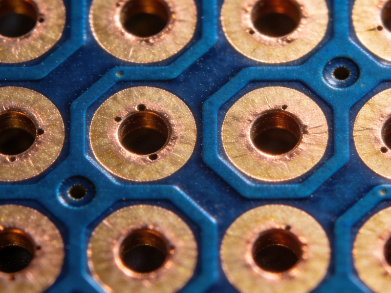
Laser Drilling and Microvias in Modern High Frequency PCB FabricationJuly/07/2026
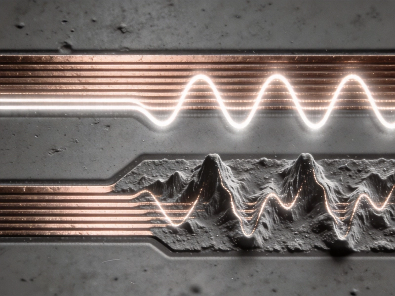
The Impact of Surface Roughness on High Frequency PCB Fabrication QualityJune/27/2026

Environmental Considerations in Sustainable High Frequency PCB FabricationSeptember/23/2026
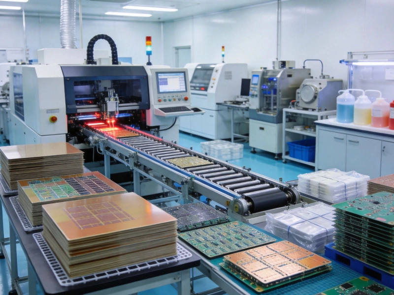
Advanced High Frequency PCB Fabrication Techniques for Low Loss PerformanceMay/29/2026
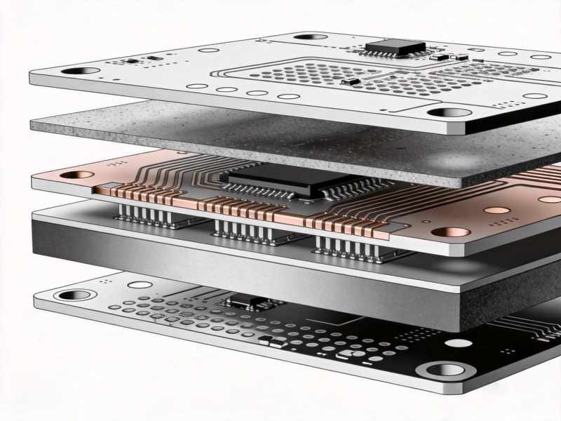
Hybrid Stack-ups: Combining FR4 and RF Materials in High Frequency PCB FabricationSeptember/14/2026