
Radio frequency and microwave applications present soldering challenges that go far beyond typical Pcb Assembly. At frequencies from several hundred megahertz to tens of gigahertz, even microscopic defects that would be irrelevant in digital circuits become critical failure points. A small void in a solder joint, a slight misalignment of a ground pad, or residual flux beneath a component can degrade Signal Integrity, increase Insertion Loss, and create impedance discontinuities that corrupt transmitted signals or corrupt received data.
The margin for error in RF assembly is razor-thin. This article examines the specific soldering defects that matter for RF performance, their root causes, and the strategies that experienced manufacturers employ to prevent them.

In digital circuits, solder joints conduct DC or low-frequency signals. The primary concerns are mechanical reliability and basic electrical continuity. A joint with a small void or slight irregularity works fine for a microcontroller or memory chip toggling at 100 MHz.
Rf Circuits operate differently. Current flows along the surface of conductors at high frequencies due to Skin Effect, concentrating at the conductor boundaries. The electromagnetic field extends beyond the physical conductor into surrounding space and adjacent features. Solder joints in Rf Circuits are not just mechanical connectors; they are Transmission Line elements whose geometry, composition, and uniformity directly affect electrical performance.
Key differences include impedance sensitivity, current distribution effects, and material compatibility. Each of these affects which defects matter and how severe they can be.
RF circuits rely on Controlled Impedance Transmission Lines to maintain Signal Integrity. Characteristic Impedance depends on the geometry of the conductor, the dielectric properties of surrounding materials, and the continuity of the ground reference. A solder joint that is too tall, too short, or irregularly shaped changes the local geometry, creating impedance discontinuities.
Reflection coefficients of even a few percent, which might seem trivial, can accumulate in complex RF systems. In a low-noise receiver front end, multiple small reflections can raise the noise floor enough to prevent detection of weak signals. In a power amplifier output stage, mismatches can cause excessive power reflection, reducing efficiency and potentially damaging components.
At RF frequencies, current flows in a thin layer near the conductor surface rather than uniformly through the cross-section. The skin depth at 10 GHz is roughly 0.8 micrometers in copper. This concentration of current means that the surface condition of conductors and solder joints matters enormously. Surface roughness, oxidation, or contamination can significantly increase effective resistance.
In solder joints, the concentration of current near the surface means that voids or inclusions near the surface affect performance more than similar defects in the bulk of the joint. The surface topology of the solder joint, including its microroughness, affects current distribution and RF loss.
The dielectric properties of solder alloys differ from the PCB laminate and from each other. At microwave frequencies, these differences affect the effective Dielectric Constant of Transmission Line structures. Solder mask over RF features, underfill beneath components, and Conformal Coating all interact with the RF fields and affect performance.
Solder that flows onto RF Transmission Lines changes their impedance and loss characteristics. Controlling solder flow during assembly is critical to maintaining the precise geometries that RF designs require.
Voids are pockets of gas trapped within solder joints during solidification. They reduce the effective cross-sectional area of the joint, affecting both mechanical strength and electrical conductivity. For RF joints, voids are particularly problematic because they alter the local dielectric environment and create inhomogeneities in the current path.
The void content of solder joints is typically expressed as a percentage of the joint area in cross-section. Industry standards allow some voiding for general assemblies, but RF applications generally require voiding below 5 to 10 percent, with some demanding below 3 percent for critical joints.
Voids arise from multiple sources: moisture in components or boards vaporizing during reflow, flux outgassing, trapped air from paste printing, and improper thermal profiles. Each source requires specific controls to minimize.
Head-in-pillow defects occur when a BGA or CSP component partially reflows onto a solder paste deposit but does not fully coalesce, leaving a gap between the component ball and the paste deposit. This defect creates an unreliable connection that may pass basic electrical testing but fail under thermal cycling or mechanical stress.
For RF assemblies, head-in-pillow defects are particularly dangerous because they create intermittent or high-resistance connections that may not be detected during test but cause field failures or performance degradation over time. The partial contact area also creates impedance discontinuities that affect RF performance.
Oxidation of component solder balls, insufficient peak temperature or time above liquidus, and improper paste selection all contribute to head-in-pillow defects. Warpage of components or substrates during reflow can also create the gaps that allow these defects to form.
Too little solder creates high-resistance connections prone to mechanical failure. Too much solder can wick onto RF transmission lines, changing their impedance and creating unintended coupling. Both conditions arise from paste printing errors, Component Placement inaccuracy, or inappropriate paste volume for the specific joint geometry.
For RF pads designed for specific paste volume, either too little or too much solder changes the coplanarity of the joint and the effective geometry of RF structures. This is particularly critical for Grounded Coplanar Waveguide and other RF transmission line formats where the spacing between signal and ground conductors determines impedance.
Pad cratering occurs when mechanical stress from testing or handling fractures the fiberglass substrate beneath copper pads, creating hairline cracks that may not be visible. Pad lift occurs when pads delaminate from the substrate, often due to excessive thermal stress during rework or repair.
For RF circuits, any disruption of the pad-to-substrate interface compromises the mechanical integrity of the joint and creates discontinuities in the ground reference. The RF fields interact with these cracks and delaminations, creating parasitic capacitances and inductances that degrade performance.
Flux residues can be conductive or capacitive, depending on their composition and cleaning. On standard digital boards, residue cleaning is important for long-term reliability but rarely affects electrical performance. On RF assemblies, residual flux in high-impedance circuits or near sensitive nodes can create parasitic capacitances that detune circuits or reduce isolation.
Flux residues in waveguide structures or near antenna feeds create losses and pattern distortions. Proper cleaning procedures, appropriate flux selection, and thorough inspection prevent contamination-related defects.
Moisture absorption by PCB laminates and components creates vapor pressure during reflow that can cause delamination, voiding, and pop-corning. For multilayer RF boards with expensive materials and complex constructions, moisture damage can be catastrophic.
Proper storage in dry cabinets or dry bags with desiccant prevents moisture absorption. Baking boards before assembly removes absorbed moisture. The baking temperature and time must be controlled to avoid damaging boards or components. Most laminate materials are baked at 125 to 130 degrees Celsius for 4 to 8 hours, though specific requirements vary.
Moisture-sensitive components, particularly area array packages, have moisture sensitivity levels that define handling and storage requirements. Components exposed to moisture and then reflowed without proper drying can crack or delaminate, creating defects that are difficult to detect.
Solder paste selection affects voiding, wetting, and process stability. No-clean pastes leave residues that may or may not be acceptable for RF applications. Water-soluble pastes provide excellent cleaning but require additional processing steps and must be thoroughly dried before subsequent operations.
For RF applications with strict voiding requirements, low-voiding solder pastes are available. These formulations are optimized to release volatiles during reflow and achieve low void content. The tradeoff is often slightly reduced wetting speed or shelf life compared to standard pastes.
Paste printing is the most significant variable in Smt assembly quality. Stencil design, printer setup, and process control all affect paste deposition accuracy and volume. For fine-pitch RF components, laser-cut stencils with appropriate aperture design achieve the best results. Squeegee condition, print speed, and pressure must be optimized for the specific paste and board characteristics.
The reflow thermal profile determines how solder melts, flows, and solidifies. A profile that is too aggressive can damage components or create voids from rapid heating. A profile that is too mild may not achieve proper melting or wetting, leading to cold joints and head-in-pillow defects.
For RF assemblies, profiles should be developed with attention to the specific board construction, component thermal mass variations, and voiding requirements. Soak zones that gradually heat boards before peak temperature help reduce thermal gradients and allow flux to prepare surfaces for wetting.
Peak temperature, time above liquidus, and cooling rate all affect final joint properties. The cooling rate influences grain structure and void content. Controlled cooling rates in nitrogen atmospheres can achieve lower voiding and better joint uniformity than air reflow.
Oxidation of component leads and solder balls increases the risk of wetting defects. Proper storage in nitrogen cabinets or sealed packaging with desiccant maintains solderability. Components should be removed from packaging only in controlled humidity environments and assembled within their floor life time after exposure.
For high-value RF components, incoming inspection of solderability helps identify components at risk. Solderability testing using wetting balance equipment quantifies how quickly and completely components wet when exposed to solder.
Rework of RF assemblies presents particular challenges. Localized heating to remove and replace components without disturbing adjacent RF structures requires specialized equipment and skilled operators. The heat from rework can reflow nearby solder joints, create thermal gradients that stress the PCB, and disturb carefully tuned RF geometries.
For complex RF boards, it is often preferable to accept lower first-pass yields rather than risk damaging adjacent structures through aggressive rework. Designing boards with replaceability in mind, including appropriate clearances and thermal relief, facilitates rework when it is necessary.
X-ray inspection reveals internal structures of solder joints that are invisible to optical inspection. BGA and QFN packages, where solder joints are hidden beneath the component, require X-ray inspection to verify joint quality. For RF assemblies, X-ray also reveals internal voids, alignment issues, and material defects that affect performance.
2D X-ray imaging shows overall joint shape and void distribution. 3D X-ray tomography provides detailed cross-sectional views that quantify void content and identify subtle defects. The choice of inspection method depends on defect types of concern, volume requirements, and budget constraints.
X-ray inspection should be performed on representative samples from each production lot, with tighter sampling for high-value assemblies. Statistical process control of X-ray results helps identify process drift before it creates defective assemblies.
Scanning acoustic microscopy (SAM) uses ultrasonic waves to detect delaminations, cracks, and voids in materials. SAM is particularly valuable for detecting delamination between PCB layers, under solder mask, and at interface boundaries that are difficult to image with X-ray.
For multilayer RF boards with critical dielectrics, acoustic imaging provides a nondestructive method to verify layer integrity before and after assembly. Delaminations in high-frequency laminates affect dielectric properties and create failures that may not appear until products are deployed.
Automated optical inspection (AOI) detects surface defects including insufficient paste, misaligned components, and solder bridging. While AOI cannot see inside joints, it identifies many defects that would otherwise require manual inspection.
For RF assemblies, AOI should include coplanarity inspection of component leads and inspection of paste deposits before reflow. Pre-reflow inspection catches printing errors before boards enter the reflow oven, reducing the risk of defects and rework.
While not a substitute for visual and X-ray inspection, electrical testing verifies circuit functionality and RF performance. Continuity testing checks for open joints. High-current testing can identify marginal connections that pass basic continuity checks. Rf Testing including vector network analysis provides the ultimate verification that assembled boards meet electrical specifications.
For high-volume RF assembly, in-circuit test fixtures combined with RF test equipment provide high-speed functional verification. The cost of test equipment and fixtures is justified by the value of detecting defects before they reach customers.
Component package selection affects assembly quality and inspection accessibility. Packages with visible solder joints, such as Gull-wing leads, are easier to inspect and rework than area array packages. For high-frequency applications requiring BGA or QFN packages, the trade-off is accepted in exchange for electrical performance benefits.
When BGA packages are necessary, consider packages with larger ball pitches that provide larger landing pads and more relaxed assembly tolerances. Packages with standoff heights that allow bottom-side inspection access simplify quality verification.
RF assemblies benefit from thermal design that promotes uniform heating during reflow. Components with significantly different thermal mass cause temperature gradients across boards, leading to inconsistent solder joint quality. Thermal simulation and thermal profiling help optimize placement and profile design.
For boards with mixed technologies including waveguide structures or precision RF components, designing for thermal symmetry helps ensure that all joints experience similar thermal histories.
Designing boards to facilitate inspection improves quality and reduces inspection time. Providing clear identification of critical joints, designing for access by inspection equipment, and including test coupons for process monitoring all contribute to effective quality control.
Test coupons with process monitor components on each panel allow verification of solderability and joint quality without consuming production boards. These coupons should be designed to reflect the thermal mass and complexity of actual production boards.
SPC techniques monitor assembly processes to identify variation before it creates defects. Monitoring paste volume from print inspections, Component Placement accuracy, and X-ray voiding results provides early warning of process drift.
Control charts for critical parameters help distinguish random variation from systematic shifts. When control charts show systematic trends, process adjustments can prevent defects before they occur.
Incoming inspection of PCBs, components, and solder paste identifies problems before they enter production. PCB inspection should verify registration, surface finish quality, and solderability. Component inspection verifies package integrity and storage condition. Solder paste inspection checks paste properties and, when necessary, reflow performance.
The scope of incoming inspection depends on supplier quality history and product value. High-value RF assemblies warrant comprehensive incoming inspection, while lower-value products may accept sampling inspection based on Supplier Qualification.
Skilled operators make a significant difference in assembly quality, particularly for challenging RF assemblies. Training programs should cover RF assembly requirements, defect identification, handling procedures, and process control responsibilities.
Certification programs that verify operator competency provide assurance that assembly is performed by qualified personnel. Periodic recertification and continuing education maintain skill levels and introduce new techniques.
When outsourcing RF assembly, clearly specify defect requirements and inspection criteria. General-purpose assembly specifications may not address the specific needs of RF circuits. Define acceptable voiding levels, inspection requirements, and any special process controls needed for your application.
Sharing design intent helps assembly partners make appropriate process decisions. Explaining which defects are critical versus cosmetic, and why, enables informed trade-offs during production.
For new RF products, collaboration during process development improves first-pass success. Sharing thermal profiles, component data sheets, and special requirements early enables process optimization before production begins.
First article inspection of prototypes reveals process sensitivities that can be addressed before production volumes begin. Building time for process refinement into development schedules prevents pressure to ship products with known quality risks.
Rf Pcb assembly demands attention to detail that goes far beyond standard Smt requirements. The defects that matter for RF performance are often invisible to cursory inspection and require sophisticated techniques to detect and prevent. Understanding which defects are critical, why they occur, and how to prevent them enables reliable high-frequency electronics manufacturing.
The keys to RF assembly success include rigorous moisture control, optimized paste selection and printing, carefully developed reflow profiles, thorough inspection using appropriate technologies, and ongoing process monitoring to catch variation before it creates defects. Working with experienced assembly partners who understand RF requirements reduces risk and improves first-pass yields.
As RF applications continue to push to higher frequencies and more compact form factors, the assembly challenges will only increase. Building expertise in RF soldering defect prevention today prepares organizations to meet the demanding requirements of next-generation wireless and microwave systems.
Acceptable voiding depends on the specific application and joint location. For most RF applications, voiding below 10 percent is acceptable, with many demanding below 5 percent. Critical joints in low-noise amplifiers or high-power amplifiers may require voiding below 3 percent. The key is to establish requirements based on RF performance impact rather than applying general industry standards.
X-ray inspection detects many critical defects including voids, misalignment, and head-in-pillow conditions. However, X-ray may not detect some subtle issues such as slight oxidation changes, microroughness variations, or contamination that affects RF performance without creating visible structural defects. Combining X-ray with other inspection methods provides more comprehensive coverage.
Lead-free solders, typically tin-silver-copper alloys, present challenges for RF assembly. They require higher reflow temperatures that may stress sensitive components. The microstructure of lead-free solders is different, with some evidence of higher voiding tendency and different wetting characteristics. For applications where RF performance is critical, tin-lead solder, where permitted, often provides better and more predictable results.
Head-in-pillow defects most commonly result from oxidation of component solder balls combined with insufficient thermal energy during reflow to break through the oxide and achieve proper wetting. Component storage conditions, moisture exposure, and reflow profile all contribute. Using fresh components, proper storage, and optimized profiles with adequate time above liquidus help prevent these defects.
Nitrogen reflow atmospheres reduce oxidation during soldering, improving wetting and reducing voiding. For RF assemblies with stringent voiding requirements, nitrogen atmosphere often provides measurable improvement in joint quality. The additional cost of nitrogen systems and gas consumption is justified when the performance benefit translates to higher yields and better RF performance.
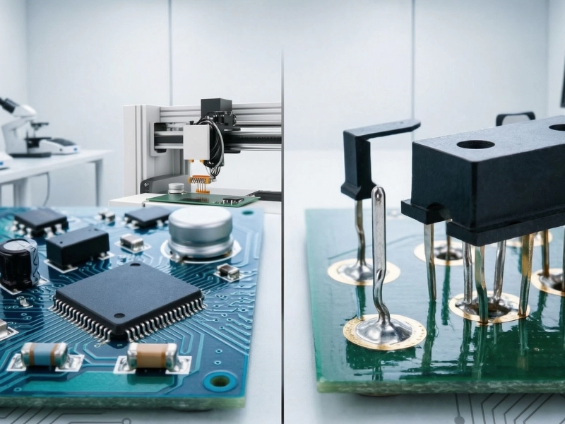
SMT vs. THT: Assembly Techniques for High Frequency PCBsJuly/03/2026

Why Component Placement is Critical in High Frequency PCB AssemblyJune/25/2026

How to Select a Turnkey High Frequency PCB Assembly PartnerAugust/06/2026

High Frequency PCB Assembly for Automotive Radar: Precision and ReliabilitySeptember/21/2026

Ensuring Signal Integrity During High Frequency PCB Assembly ProcessesJuly/15/2026

The Challenges of High Frequency PCB Assembly: Handling Sensitive ComponentsMay/29/2026

High Frequency PCB Assembly Best Practices for 5G and RF ModulesJune/08/2026

Why Advanced Testing Equipment Defines Top High Frequency PCB CapabilitiesJuly/07/2026