As 5G networks expand globally and RF applications multiply across industries, High Frequency Pcb Assembly has become increasingly critical. Manufacturing reliable 5G and RF modules demands specialized knowledge that goes far beyond standard Pcb Assembly practices. This comprehensive guide explores the best practices Chinese manufacturers employ to ensure Signal Integrity, minimize losses, and maintain consistent performance in high-frequency applications.
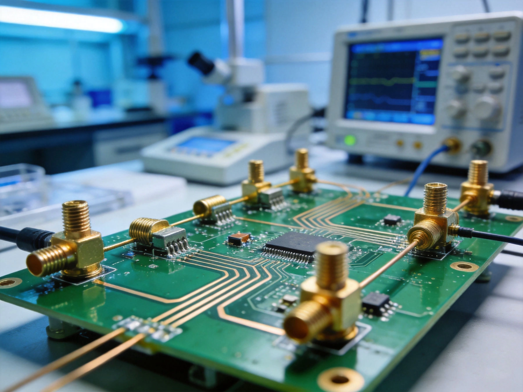
High Frequency Pcb Assembly presents unique challenges that don't exist in conventional electronics manufacturing. When dealing with frequencies above 1 GHz—typical for 5G applications ranging from sub-6 GHz to millimeter-wave bands—every design decision impacts performance.
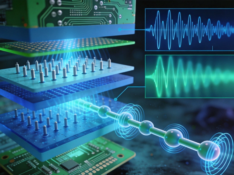
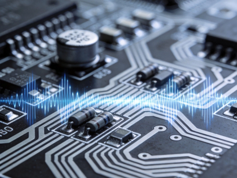
At microwave frequencies, PCB traces behave as transmission lines rather than simple conductors. Signal Integrity depends on controlling:
Standard Fr-4 materials prove inadequate for high-frequency applications. Leading Chinese PCB manufacturers recommend specialized laminates:
Key material properties to evaluate include Dielectric Constant (Dk), Dissipation Factor (Df), coefficient of thermal expansion (CTE), and moisture absorption rates.
Successful High Frequency Pcb assembly begins with proper design. These guidelines help ensure manufacturability while maintaining RF performance:
Proper transmission line implementation forms the foundation of Rf Pcb design:
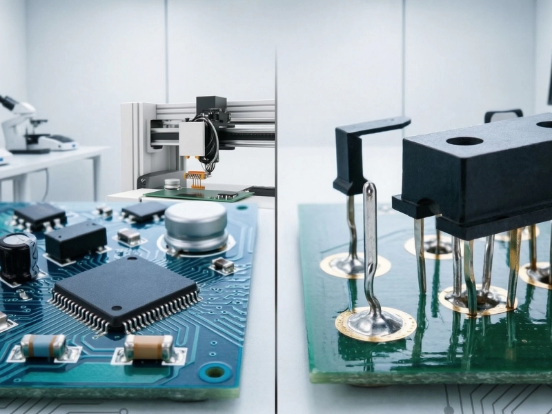
Strategic Component Placement dramatically affects High Frequency Pcb assembly outcomes:
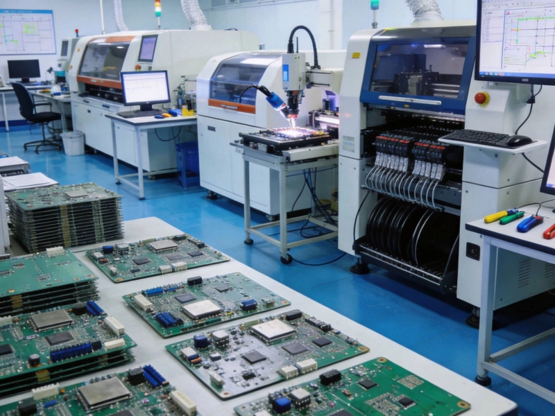
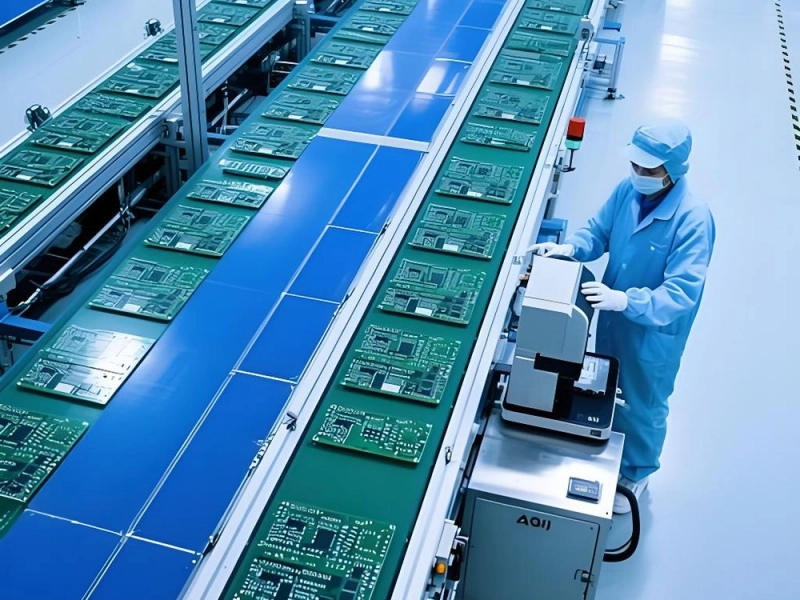
High frequency Pcb Assembly demands precision at every manufacturing stage. Chinese manufacturers with 5G experience follow these critical practices:
Proper solder paste application prevents common RF assembly defects:
Temperature profiles significantly impact RF component reliability:
RF components require special handling during high frequency PCB assembly:
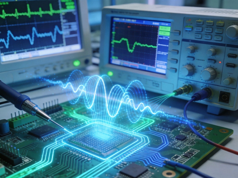
Comprehensive testing ensures high frequency PCB assembly meets performance specifications:
Even experienced manufacturers encounter challenges with RF assemblies. Avoid these common mistakes:
China's electronics manufacturing ecosystem offers significant advantages for high frequency PCB assembly:
When selecting a manufacturing partner, verify their capabilities through:
The evolution of 5G and emerging wireless technologies drives continuous improvement in RF assembly:
High frequency PCB assembly for 5G and RF modules requires specialized expertise spanning materials science, Precision Manufacturing, and RF engineering. By following the best practices outlined in this guide—selecting appropriate materials, optimizing designs for manufacturability, controlling assembly processes precisely, and implementing comprehensive testing—you can achieve reliable performance in demanding wireless applications.
Partnering with experienced Chinese manufacturers provides access to world-class capabilities while maintaining cost competitiveness. As 5G networks continue expanding and new RF applications emerge, mastering these assembly best practices positions your products for success in the high-frequency future.
Ready to manufacture your 5G or RF module? Contact our engineering team for a comprehensive Dfm review and competitive quotation tailored to your specific high frequency PCB assembly requirements.
High frequency assembly requires specialized materials with low dielectric loss, precise Impedance Control, and careful handling of sensitive RF components. Standard Fr-4 materials and conventional assembly practices often prove inadequate for frequencies above 1 GHz.
Rogers RO4000 series, Taconic TLY materials, and Arlon AD laminates are popular choices for 5G applications. Material selection depends on specific frequency ranges, with millimeter-wave applications requiring the lowest loss materials available.
Maintain consistent trace widths, use appropriate stackup designs with solid ground planes, work closely with your manufacturer to verify dielectric constants, and specify Impedance Control requirements clearly in fabrication drawings.
Network analyzer measurements for S-parameters, TDR for impedance verification, power handling tests for amplifiers, and environmental testing for reliability validation are essential for ensuring Rf Pcb performance.
While standard Smt equipment can place many RF components, high frequency PCB assembly benefits from placement machines with higher accuracy (±0.05mm), specialized nozzles for delicate components, and controlled atmosphere reflow systems.
Ensuring Signal Integrity During High Frequency PCB Assembly ProcessesJuly/15/2026
The Challenges of High Frequency PCB Assembly: Handling Sensitive ComponentsMay/29/2026
Why Component Placement is Critical in High Frequency PCB AssemblyJune/25/2026
SMT vs. THT: Assembly Techniques for High Frequency PCBsJuly/03/2026
How Dielectric Constant (Dk) and Loss Factor (Df) Affect High Frequency PCB MaterialsJuly/18/2026
High Frequency PCB Knowledge: How to Minimize Insertion Loss and ReflectionJuly/21/2026
The Benefits of Rapid High Frequency PCB PrototypingMay/29/2026
7 Key Factors to Consider When Choosing a High Frequency PCB ManufacturerMay/29/2026