Open Nav

The terms "high-speed" and "high-frequency" are used interchangeably in many PCB design discussions, and the confusion is understandable—both involve fast signals, both demand Controlled Impedance, and both are sensitive to material properties and layout geometry. But they describe fundamentally different design paradigms with distinct failure modes, material requirements, simulation approaches, and validation methods. Conflating the two leads to over-designed RF boards (wasting money on PTFE laminates where Megtron6 suffices) or under-designed digital interconnects (using FR4 where the eye diagram has already collapsed). Understanding the difference between high-speed and high-frequency PCB design—and knowing when each applies—is essential knowledge for any engineer working on modern electronics.

The distinction starts with how we characterize the signal itself.
In digital design, "high-speed" refers to signals where the transition time (rise/fall time) is fast enough that Transmission Line effects become significant. The critical metric is not the clock frequency or data rate—it is how quickly the signal transitions between logic levels.
A 1 MHz clock with 1 ns rise time is a high-speed signal. A 100 MHz clock with 100 ns rise time is not. The reason: a fast edge contains high-frequency spectral content regardless of the fundamental frequency. A 1 ns rise time has significant energy up to approximately 350 MHz (using the 0.35/tr approximation), and that high-frequency content interacts with the PCB interconnect as a Transmission Line.
The threshold for "high-speed" is typically defined by the relationship between the signal transition time and the propagation delay across the interconnect. When the round-trip propagation delay exceeds the signal transition time, the interconnect behaves as a transmission line rather than a lumped circuit—and high-speed design rules (Impedance Matching, termination, length matching) must be applied.
In RF and microwave design, "high-frequency" refers to signals where the carrier frequency or operating frequency is high enough that the PCB material's dielectric properties significantly affect signal propagation. The concern is not logic transitions but continuous-wave or modulated RF energy.
High-frequency design cares about Insertion Loss, return loss, phase linearity, and radiation efficiency—parameters that describe how the PCB medium affects the RF signal as it propagates. A 28 GHz 5G carrier, a 77 GHz Automotive Radar signal, and a 2.4 GHz WiFi signal are all high-frequency signals, even though their modulation bandwidths differ dramatically.
The threshold for "high-frequency" is application-dependent and somewhat subjective, but a practical definition is: any signal where the PCB laminate's Dissipation Factor (Df) contributes more than 0.5 dB of Insertion Loss per inch of trace is operating in the high-frequency regime.
Beyond the definitions, high-speed and high-frequency design differ in their core engineering philosophy—what they are trying to optimize and what failure modes they are trying to prevent.
High-speed digital design is fundamentally about timing and Signal Integrity. The goal is to ensure that digital signals arrive at their destination with:
The key failure mode is logic error: the receiver misinterprets a bit because the eye diagram has closed, a setup/hold time has been violated, or crosstalk has pushed a quiet signal past the threshold. The PCB designer's job is to keep the eye open.
High-frequency design is fundamentally about power transfer and signal fidelity in the frequency domain. The goal is to ensure that RF signals propagate with:
The key failure mode is link budget failure: the signal-to-noise ratio at the receiver is insufficient to demodulate the signal, the antenna efficiency is too low to close the link, or spurious coupling has corrupted the frequency plan. The PCB designer's job is to minimize loss and preserve the RF energy.
Material selection is where the high-speed versus high-frequency distinction has the most practical impact on PCB design decisions and cost.
For high-speed digital signals, the primary material concern is insertion loss at the frequencies contained in the signal's spectral content. A PCIe Gen5 signal at 32 GT/s has a Nyquist frequency of 16 GHz, but most of the energy that determines eye diagram quality is below 8–10 GHz. At these frequencies:
The secondary material concern for high-speed design is Dk uniformity for Impedance Control. Differential impedance must typically be controlled to ±10% (100Ω ± 10Ω) for high-speed serial links. Low-loss FR4 variants with controlled Dk specifications (±0.04 or better) meet this requirement without resorting to RF-grade materials.
For high-frequency RF signals, the material requirements are more stringent because the operating frequency is higher and the loss budgets are tighter:
Both high-speed and high-frequency design require Impedance Control, but with different tolerance requirements and different consequences for being out of tolerance.
High-speed serial links (PCIe, USB, SATA, Ethernet) specify differential impedance targets with typical tolerances of ±10%:
Being out of tolerance causes reflections that reduce the eye diagram height and increase jitter, but the link typically still operates with some margin reduction. Equalization in the SerDes (CTLE, DFE) can partially compensate for impedance discontinuity effects. The consequence of impedance violation is degraded performance, not complete failure.
RF Impedance Matching is typically much tighter because it directly affects power transfer efficiency:
Being out of tolerance causes direct power loss—a 10% impedance mismatch creates 0.2 dB return loss, reducing delivered power and degrading the entire RF chain's noise figure. There is no equalization to compensate. The consequence of impedance violation is link budget failure—missed sensitivity, reduced range, or failed compliance testing.
Via design illustrates another practical difference between the two paradigms.
For high-speed digital signals, the primary via concern is via stubs. When a signal transitions from an outer layer to an inner layer using a through-hole via, the unused portion of the via barrel (the stub) creates a resonant cavity that causes notch-shaped insertion loss at the stub resonance frequency. For a 10-layer board with a 0.1-inch stub, the resonance occurs at approximately 15 GHz—directly in the band of PCIe Gen5 and USB4 signals.
Solutions include back-drilling (controlled-depth drilling to remove the stub), HDI blind/buried vias (which have no stub by construction), and via transitions optimized for impedance continuity. These are well-understood techniques with established design rules.
For RF signals, via design is more nuanced because vias serve multiple purposes in Rf Circuits:
The simulation and measurement approaches for high-speed and high-frequency PCBs differ substantially.
Some layout rules are shared between high-speed and high-frequency design, while others are specific to one paradigm.
Modern electronics increasingly contain both high-speed digital and high-frequency RF circuitry on the same board. A 5G smartphone has a multi-Gbps digital bus to the modem and 28 GHz mmWave RF front-ends. A radar processor board has PCIe Gen4 backplane interfaces and 77 GHz RF channels. These mixed designs require understanding both paradigms and managing their interaction.
The most effective approach is physical partitioning: separate the board into digital and RF zones with a ground plane barrier between them. The digital section uses cost-optimized low-loss FR4 material, conventional via construction, and standard design rules. The RF section uses Rogers or PTFE laminates, microvia construction, and RF-specific layout rules. The ground plane separation provides isolation, and the material boundary is placed at a layer interface where a continuous ground plane acts as both an EMI shield and a material transition boundary.
Even with partitioning, some challenges span both domains:
The conflation of high-speed and high-frequency design creates several persistent misconceptions:
A 112 Gbps PAM4 signal has a Nyquist frequency of 28 GHz, but its signal bandwidth (the frequency range containing most of the energy that determines receiver performance) extends to approximately 40–50 GHz including harmonics. This bandwidth is comparable to mmWave RF, and the material requirements are indeed similar. However, the design approach differs: the digital engineer cares about eye diagram metrics (insertion loss to a specified mask, return loss, crosstalk as a voltage margin reduction), while the RF engineer cares about S-parameters as power ratios (insertion loss in dB, return loss in dB, isolation in dB). Same frequencies, different optimization targets.
Using Rogers RO4003C for a PCIe Gen5 link does reduce insertion loss compared to Megtron6—but the improvement (perhaps 0.1–0.2 dB/inch) rarely justifies the 3–5× material cost premium. High-speed links have loss budgets that can be met with appropriate low-loss FR4 variants plus equalization. Rf Materials are justified only when the loss budget cannot be met with lower-cost alternatives.
A ±10% impedance tolerance that is adequate for high-speed digital may be completely inadequate for an RF matching network or antenna feed. The appropriate tolerance depends on the application's sensitivity to reflection—not on the signal frequency alone.
In high-speed digital, crosstalk reduces voltage margin and timing margin—it is a performance degradation. In Rf Design, crosstalk can cause receiver desensitization (increased noise floor), transmitter spurious emissions (regulatory failure), and oscillator pulling (complete functional failure). The consequences of crosstalk in RF are often binary: the system either meets its frequency plan or it does not. This difference in failure severity means RF designs require more aggressive isolation measures (via fencing, separate ground domains, physical partitioning) than digital designs with similar trace spacing.
High-speed digital design and high-frequency Rf Design share a common foundation in transmission line theory, impedance control, and electromagnetic awareness. But they diverge in their optimization targets, material requirements, design rules, simulation approaches, and failure modes. High-speed design optimizes for timing margin and voltage margin in the time domain, using loss-controlled FR4 variants and eye diagram metrics. High-frequency design optimizes for power transfer and signal fidelity in the frequency domain, using low-Df RF laminates and S-parameter metrics.
Understanding this distinction is not academic—it directly affects material cost, design effort, simulation methodology, and manufacturing yield. Choosing RF-grade materials for a digital-only board wastes cost. Choosing digital-grade materials for an RF board fails the link budget. And when both paradigms coexist on the same board, only engineers who understand both can partition the design effectively, specify materials correctly, and validate the complete system.
For hardware teams that need guidance navigating the high-speed versus high-frequency material and design decision, consulting with an experienced PCB manufacturer early in the design process can prevent costly material mis-specification and identify the optimal construction approach for boards that span both domains.
In terms of spectral content, yes—a 10 Gbps NRZ signal has significant energy to approximately 15–20 GHz. However, the design approach remains high-speed (time-domain) rather than high-frequency (frequency-domain) because the optimization target is eye diagram quality, not power transfer efficiency. The material selection may overlap (both may need low-Df laminates), but the design rules, simulation approach, and validation methodology differ.
Use Rogers RO4003C or equivalent when the signal's insertion loss on Megtron6 exceeds the link budget. For high-speed digital links (PCIe Gen5, 400GbE), calculate the total channel loss on Megtron6 and compare it to the protocol's loss specification. If margin remains, Megtron6 is sufficient. For RF applications, compute the insertion loss at the carrier frequency—if Megtron6's loss exceeds the allocated budget for the PCB trace section, upgrade to Rogers. For most Sub-6 GHz RF with trace lengths under 2 inches, Megtron6 may suffice. For mmWave or long RF traces, Rogers or PTFE is typically needed.
For most high-speed digital interconnects, 2D or 2.5D field solvers (such as those built into EDA tools like HyperLynx, SIwave, or Sigrity) provide sufficient accuracy for impedance calculation and loss estimation. 3D EM simulation (HFSS, CST) is needed only for structures where full-wave effects are significant—via transitions at very high frequencies (above 20 GHz), connector breakout regions, and areas with significant radiation. For RF designs, 3D EM simulation is standard practice for any structure that is not a simple uniform transmission line.
Yes, but with caveats. A fabricator that processes standard low-loss FR4 for high-speed digital boards may lack the equipment and expertise for Rogers or PTFE laminates (which require different drilling parameters, plating processes, and lamination recipes). Conversely, an RF-specialist fabricator may not have the high-volume production lines needed for cost-competitive digital boards. For mixed high-speed/high-frequency boards, select a fabricator that demonstrably supports both material systems and has experience with mixed-material lamination.
Inadequate isolation between digital and RF sections. Engineers often route digital traces too close to RF circuitry or share ground planes without proper partitioning, allowing digital switching noise to couple into sensitive RF paths. The result is elevated phase noise, degraded receiver sensitivity, or spurious emissions. The fix is always the same: physical partitioning with ground plane barriers and keep-out zones around RF circuitry—but it must be implmented from the beginning of the layout, not added as an afterthought.
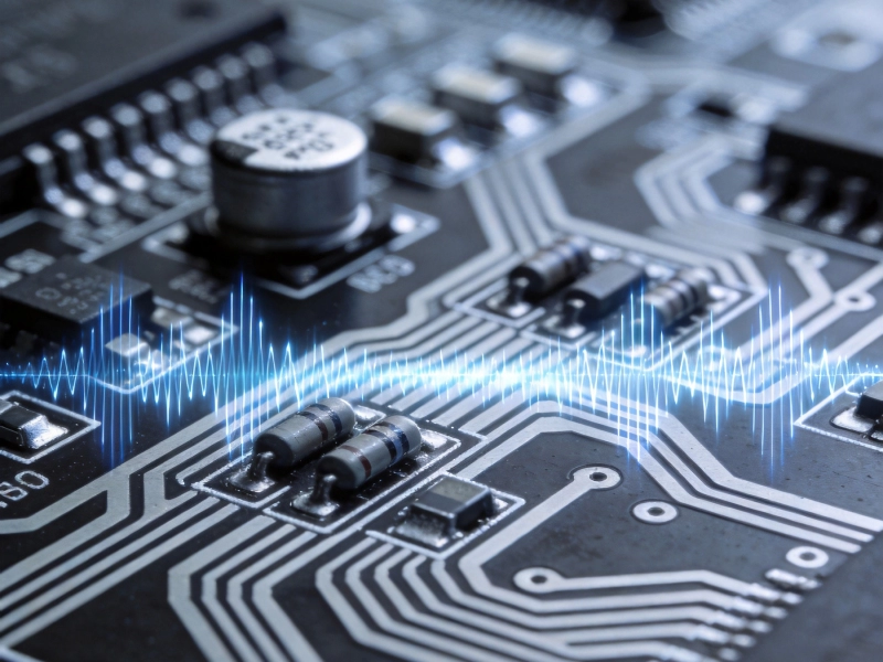
High Frequency PCB Knowledge: How to Minimize Insertion Loss and ReflectionJuly/21/2026
High Frequency PCB Knowledge: Managing Crosstalk and EMI in Dense LayoutsAugust/11/2026
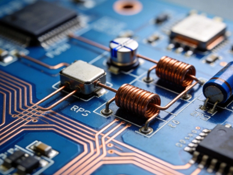
Key High Frequency PCB Knowledge for Successful RF Circuit DesignSeptember/07/2026
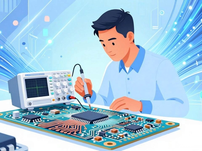
Essential High Frequency PCB Knowledge for Hardware Engineers and DesignersJune/15/2026
The Engineer's Guide to High Frequency PCB Knowledge and Stack-up DesignJuly/31/2026
Demystifying Impedance Control: Core High Frequency PCB KnowledgeJuly/09/2026
Essential High Frequency PCB Knowledge for Hardware Engineers and DesignersMay/29/2026
High Frequency PCB Applications in Satellite Communication and AerospaceJuly/22/2026