
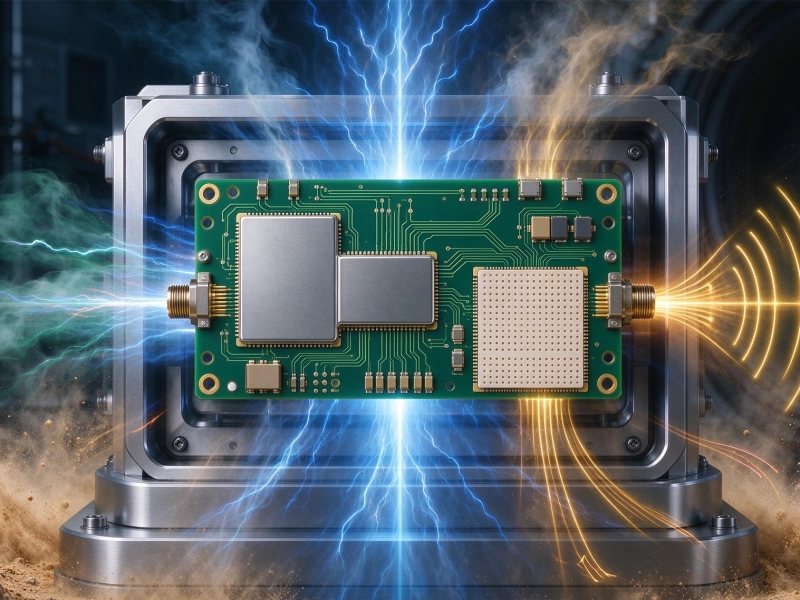
High frequency printed circuit boards have become the backbone of modern satellite communication and aerospace systems, enabling the transmission of vast amounts of data across vast distances with remarkable precision and reliability. As satellite networks expand to provide global connectivity, Earth observation capabilities, and deep space exploration, the demands on high frequency PCB technology continue to escalate. These specialized circuit boards must operate flawlessly in the harshest environments imaginable—from the vacuum of space to the intense vibrations of launch—while maintaining Signal Integrity at frequencies that can exceed 100 GHz.
The unique challenges of satellite and aerospace applications drive innovations in high frequency PCB design, material science, and manufacturing processes. Understanding these applications and their requirements helps engineers develop solutions that meet the stringent demands of space-based communication systems while pushing the boundaries of what's possible in high frequency electronics.
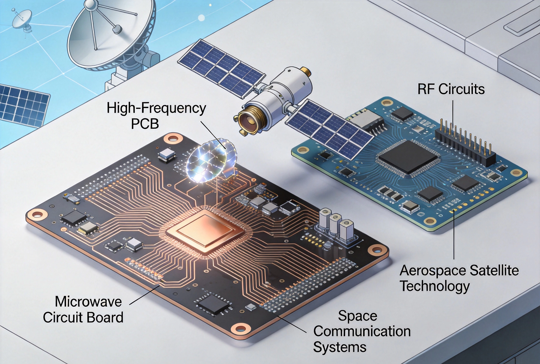
Satellite communication systems rely heavily on high frequency PCBs for virtually every aspect of their operation. From the initial signal processing to final transmission and reception, these specialized circuit boards form the electronic nervous system that enables satellites to fulfill their missions.
Satellite transponders represent one of the most critical high frequency pcb applications in space systems. These systems receive uplink signals from ground stations, process them through frequency conversion and amplification, and retransmit them back to Earth. High frequency PCBs in transponder systems must handle multiple frequency bands simultaneously, often ranging from L-band (1-2 GHz) through Ku-band (12-18 GHz) and extending to Ka-band (26.5-40 GHz) and beyond for high-throughput satellites.
The transponder's signal path requires extremely low loss and precise Impedance Control to maintain signal quality. Any degradation in the signal path translates directly to reduced data throughput, increased error rates, or complete communication failure. High frequency PCBs in these applications typically use specialized materials with low Dielectric Constant (Dk) and low Dissipation Factor (Df) to minimize Signal Loss and maintain Signal Integrity across the frequency spectrum.
Modern satellites increasingly employ phased array antennas and active beamforming systems that require sophisticated high frequency PCBs. These systems use multiple antenna elements with precise phase and amplitude control to steer beams electronically, enabling a single satellite to serve multiple coverage areas simultaneously without mechanical steering.
High frequency PCBs in antenna systems integrate RF distribution networks, phase shifters, power amplifiers, and control electronics into compact, lightweight packages. The RF distribution networks must maintain precise phase relationships across multiple paths, requiring careful attention to trace length matching, Impedance Control, and isolation between channels. Materials with stable dielectric properties across temperature ranges become essential for maintaining beam pointing accuracy as satellites experience thermal cycling in orbit.
Advanced satellites incorporate onboard digital processing and switching capabilities that require high frequency PCBs for interconnection between processing elements, memory systems, and RF front-ends. These digital backplanes must support high-speed serial interfaces operating at multi-gigabit per second data rates, demanding careful attention to signal integrity, crosstalk management, and power distribution.
The combination of high-speed digital signals and sensitive Rf Circuits on the same board creates significant design challenges. High frequency PCBs must provide adequate isolation between noisy digital sections and sensitive analog RF sections while maintaining the compact form factors required for space applications.
Beyond Satellite Communications, high frequency PCBs play crucial roles in aerospace radar, electronic warfare, and remote sensing systems:
SAR systems used in Earth observation satellites and reconnaissance aircraft require high frequency PCBs for their transmit/receive modules, signal processing electronics, and beam steering controls. These systems operate at microwave frequencies typically ranging from 1 GHz to 40 GHz, with X-band (8-12 GHz) and Ku-band being particularly common for high-resolution imaging.
The T/R modules in SAR systems present unique challenges for high frequency pcb design. Each module combines power amplifiers, low noise amplifiers, phase shifters, and switches in a compact package that must operate reliably under extreme environmental conditions. Thermal Management becomes critical as these modules generate significant heat while operating in the vacuum of space where conventional cooling methods are unavailable.
Weather satellites and research aircraft carry sophisticated radar systems for atmospheric profiling and precipitation measurement. These systems operate at frequencies optimized for detecting specific atmospheric constituents—typically around 13.6 GHz for precipitation radar and 94 GHz for cloud profiling radar. High frequency PCBs in these applications must maintain calibration stability across wide temperature ranges and provide the phase stability necessary for coherent signal processing.
Military aerospace platforms rely on high frequency PCBs for electronic warfare applications including radar warning receivers, electronic countermeasures, and signals intelligence systems. These applications span an extremely wide frequency range, often from 500 MHz to 40 GHz or higher, requiring broadband performance from Rf Circuits.
The dense packaging requirements of modern electronic warfare systems push High Frequency Pcb technology to its limits. Multiple RF channels must coexist in minimal space while maintaining isolation to prevent self-interference and ensure system sensitivity. Advanced materials and sophisticated layout techniques enable the integration density required for these applications.
The Extreme Environment of space imposes stringent requirements on Pcb Materials that go far beyond typical terrestrial applications:
Signal Loss in high frequency circuits increases with frequency, making Low-loss Materials essential for space applications where every decibel of signal strength matters. Space-grade high frequency PCBs typically use materials with dissipation factors below 0.002 at operating frequencies to minimize Insertion Loss.
Ptfe-based laminates like Rogers RT/duroid and Taconic TLY materials provide excellent low-loss characteristics for frequencies up to millimeter-wave ranges. These materials offer dissipation factors as low as 0.0009, enabling long signal paths with minimal attenuation. However, Ptfe's high coefficient of thermal expansion and processing challenges require careful design and manufacturing approaches.
Ceramic-filled hydrocarbon materials like Rogers RO4000 series provide a compromise between low loss and easier processing. These materials offer good high-frequency performance with more manageable thermal expansion characteristics and better compatibility with standard Pcb Manufacturing processes.
Satellites experience extreme thermal cycling as they move between sunlight and eclipse, with temperatures ranging from -150°C to +150°C depending on orbit and thermal control systems. Pcb Materials must maintain stable dielectric properties across this entire temperature range to ensure consistent RF performance.
Dielectric Constant variation with temperature directly affects circuit performance—changes in Dk alter Transmission Line impedance, filter center frequencies, and antenna resonant frequencies. Materials with low temperature coefficient of dielectric constant (TCDk) are essential for maintaining calibration and performance stability. Advanced materials like Rogers TMM and certain ceramic-filled hydrocarbons offer TCDk values near zero, providing excellent thermal stability.
Materials used in space must have minimal outgassing—release of volatile compounds in vacuum—that could contaminate optical surfaces, thermal control surfaces, or other sensitive spacecraft components. NASA and ESA specify maximum total mass loss (TML) and collected volatile condensable materials (CVCM) limits for spaceflight materials.
Standard Fr-4 and many commercial PCB materials exceed outgassing limits and cannot be used in space applications. Space-qualified materials undergo extensive testing to verify outgassing characteristics. PTFE materials generally exhibit low outgassing, while ceramic-filled materials may require specific formulations to meet space requirements.
Space radiation—including trapped particles in the Van Allen belts, solar particle events, and galactic cosmic rays—can degrade PCB materials over time. Total ionizing dose (TID) accumulation can alter dielectric properties, potentially changing circuit performance during the mission lifetime.
Materials with radiation-resistant properties help maintain consistent performance throughout extended missions. PTFE and many ceramic-filled materials show good radiation resistance, while some hydrocarbon-based materials may experience more significant degradation. Material selection must consider the expected radiation environment and mission duration.
Launch vibrations and deployment shocks impose severe mechanical stresses on PCB assemblies. Materials must have adequate mechanical strength to survive these stresses while maintaining electrical performance. Coefficient of thermal expansion (CTE) matching between materials is critical to prevent delamination or via cracking under thermal cycling.
Materials with CTE values close to copper (approximately 17 ppm/°C) help minimize stress at plated through-holes and vias. Ceramic-filled materials can be formulated with CTE values matching copper more closely than pure PTFE, improving reliability in multilayer constructions.
Designing high frequency PCBs for satellite and aerospace applications requires attention to details that might be less critical in terrestrial applications:
Maintaining precise Controlled Impedance is essential for high frequency signal integrity. Impedance mismatches cause reflections that degrade signal quality and reduce power transfer efficiency. Space applications typically require impedance tolerances of ±5% or better, with some critical applications demanding ±2%.
Achieving these tolerances requires careful attention to dielectric thickness control, trace width consistency, and material property uniformity. High Frequency Pcb manufacturers use specialized processes including controlled-depth routing, laser direct imaging, and precision etching to maintain the tight tolerances required.
Transmission Lines in space applications must be designed for the specific frequency ranges and power levels involved. Microstrip and stripline configurations are most common, with substrate thickness and trace geometry optimized for the target impedance and frequency range.
For very high frequencies, coplanar waveguide structures may provide better performance than traditional Microstrip, offering improved isolation and reduced dispersion. However, coplanar waveguide requires more complex fabrication and may be more sensitive to manufacturing variations.
Vias represent discontinuities in Transmission Lines that can cause impedance variations and signal reflections at high frequencies. Via optimization techniques include:
High frequency circuits are sensitive to power supply noise and impedance. Power distribution networks must provide clean power with low impedance across the entire frequency range of operation. This requires:
Heat dissipation in space is challenging because convection cooling is unavailable in vacuum. High frequency PCBs must be designed to conduct heat effectively to mounting surfaces or dedicated Thermal Management systems. Thermal vias, metal-backed substrates, and careful Component Placement all contribute to effective thermal management.
Power amplifiers and other heat-generating components require particular attention. Thermal modeling and analysis help ensure that peak temperatures remain within safe operating limits across the expected thermal environment. Materials with higher thermal conductivity can help spread heat more effectively, though this must be balanced against electrical performance requirements.
Manufacturing high frequency PCBs for space applications involves specialized processes and stringent quality control:
High Frequency Materials often require special handling to maintain properties and prevent contamination. PTFE materials, in particular, are softer and more dimensionally sensitive than standard Fr-4, requiring careful processing to maintain registration and dimensional stability. Material storage conditions must prevent moisture absorption that could affect dielectric properties or cause delamination during lamination.
High frequency circuits often require very fine features with tight tolerances. Trace width control is critical for maintaining impedance, with tolerances of ±0.0005 inches or better sometimes required. Advanced etching processes including pulse plating, differential etching, and laser direct imaging help achieve the precision needed for space-grade high frequency PCBs.
Plated through-holes and vias must have uniform copper plating with adequate thickness to handle current requirements and survive thermal cycling. In space applications, via reliability is critical—failures in RF vias can disable entire communication channels. High aspect ratio plating, controlled-depth drilling, and careful process control ensure reliable via performance.
Surface finish selection affects both solderability and high frequency performance. Electroless nickel immersion gold (ENIG) provides excellent shelf life and solderability but introduces nickel's magnetic properties and Skin Effect losses at high frequencies. Immersion silver offers lower loss but requires careful handling to prevent tarnishing. Electroplated gold over nickel provides the best high frequency performance but at higher cost.
Space-grade high frequency PCBs undergo extensive quality verification including:
Several technology trends are shaping the future of high frequency PCBs in satellite and aerospace applications:
Satellite systems are pushing toward higher frequencies to access wider bandwidths and avoid spectrum congestion. Q-band (33-50 GHz) and V-band (50-75 GHz) operations are becoming more common for high-throughput satellites and inter-satellite links. These higher frequencies place even greater demands on PCB materials and manufacturing processes, driving development of materials with lower loss and better high-frequency characteristics.
Software-defined radio (SDR) architectures are replacing traditional hardware-defined transponders, enabling satellites to reconfigure their communication parameters through software updates rather than hardware changes. SDR systems require high frequency PCBs that can support wide frequency ranges with reconfigurable filtering and signal processing, placing new demands on broadband performance and flexibility.
Electronically steerable phased arrays are becoming standard for both commercial and military satellites, replacing traditional parabolic reflectors. These systems require massive numbers of high frequency PCBs for their T/R modules, driving demand for cost-effective manufacturing of space-grade high frequency circuits at higher volumes than traditional satellite applications.
CubeSats and other small satellite platforms demand ever-smaller, lighter electronics packages. High frequency PCBs must integrate more functionality into smaller spaces while maintaining performance and reliability. Advanced packaging techniques including system-in-package (SiP) and 3D integration are being applied to high frequency space electronics to achieve the required density.
For extremely high data rates, optical interconnects are beginning to complement or replace electrical high frequency connections within satellites. High frequency PCBs must integrate both electrical and optical components, requiring new design approaches and manufacturing techniques for hybrid electro-optical assemblies.
Rigorous testing ensures that high frequency PCBs will perform reliably in space:
Comprehensive electrical testing validates that PCBs meet all performance specifications:
Environmental testing validates that PCBs survive the space environment:
For extended missions, long-term reliability assessment predicts performance over the mission lifetime:
High frequency PCBs are fundamental enablers of modern satellite communication and aerospace systems, providing the electronic infrastructure that makes global connectivity, Earth observation, and space exploration possible. The unique demands of space applications—extreme environments, zero-failure tolerance, and extended mission lifetimes—drive continuous innovation in materials, design techniques, and manufacturing processes.
As satellite constellations expand, data rates increase, and new applications emerge, the importance of high frequency PCB technology in space systems only grows. Success in this demanding field requires deep understanding of RF engineering principles, materials science, and space environment effects, combined with meticulous attention to design details and Manufacturing Quality.
The future of satellite communication depends on continued advances in high frequency PCB technology—enabling higher frequencies, greater bandwidth, improved reliability, and reduced cost. For engineers working in this field, the challenges are significant, but so are the rewards of contributing to humanity's expansion into space and the global connectivity that satellite systems provide.
Satellite communication PCBs span a wide range of frequencies depending on the application. L-band (1-2 GHz) is common for mobile satellite services, S-band (2-4 GHz) for some navigation and weather systems, C-band (4-8 GHz) for traditional fixed satellite services, Ku-band (12-18 GHz) for direct broadcast satellite and VSAT, and Ka-band (26.5-40 GHz) for high-throughput satellites. Emerging systems are pushing into Q-band (33-50 GHz) and V-band (50-75 GHz) for even higher capacity.
Standard FR-4 has several limitations that make it unsuitable for space high frequency applications. Its relatively high Dissipation Factor (typically 0.020 or higher) causes excessive signal loss at microwave frequencies. FR-4 also exhibits significant variation in dielectric constant with temperature and moisture absorption, causing performance instability. Additionally, most FR-4 formulations exceed outgassing limits for space applications. Space-grade high frequency PCBs use specialized materials like PTFE or ceramic-filled hydrocarbons that provide low loss, thermal stability, and low outgassing.
Space radiation can affect high frequency PCBs through several mechanisms. Total ionizing dose (TID) accumulation can gradually change dielectric properties, potentially altering Transmission Line impedance and filter characteristics. Radiation can also cause darkening of some Dielectric Materials, increasing loss at optical wavelengths used in fiber optic systems. Single event effects from heavy ions can cause temporary disruptions in active circuits. Material selection and Shielding help mitigate these effects, with radiation-resistant materials and appropriate Shielding design maintaining performance throughout mission lifetimes.
Mission life requirements vary significantly depending on the satellite application. Low Earth orbit (LEO) satellites for communications constellations may have design lives of 5-7 years, reflecting the relatively harsh radiation environment at lower altitudes and the need for constellation refresh. Geostationary communications satellites typically require 15-year design lives to justify their high launch costs. Scientific spacecraft and deep space probes may require even longer lifetimes, sometimes 20+ years. These extended lifetimes drive the rigorous qualification requirements and conservative design margins used in space-grade high frequency PCBs.
Thermal cycling requirements drive several aspects of High Frequency Pcb Design. Material selection must consider coefficient of thermal expansion (CTE) matching to prevent via cracking and delamination. Layer stackups are designed to be symmetrical to minimize board warpage. Via designs use filled and capped vias to improve reliability under thermal stress. Trace designs incorporate features like teardrop connections to distribute thermal stress. Component mounting must accommodate thermal expansion without stressing solder joints. All these considerations ensure that RF performance remains stable despite the extreme thermal cycling experienced in orbit.
Top High Frequency PCB Applications in the 5G and Telecommunications IndustryJune/16/2026
The Role of High Frequency PCB Applications in Autonomous Driving and ADASJuly/10/2026
High Frequency PCB Materials for Automotive Radar: Durability and SpeedSeptember/26/2026
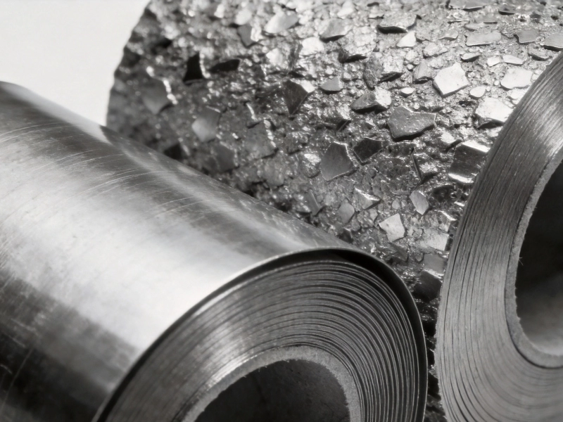
The Impact of Copper Foil Type on High Frequency PCB Materials PerformanceSeptember/16/2026
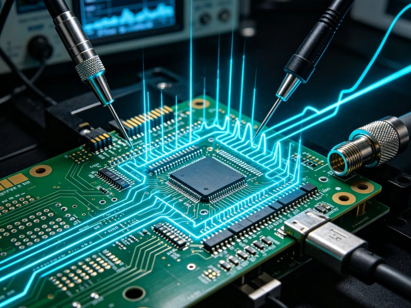
The Importance of Impedance Control in Our High Frequency PCB CapabilitiesSeptember/03/2026
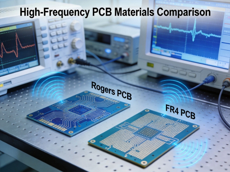
Rogers vs. FR4: Choosing the Right High Frequency PCB MaterialsJune/12/2026
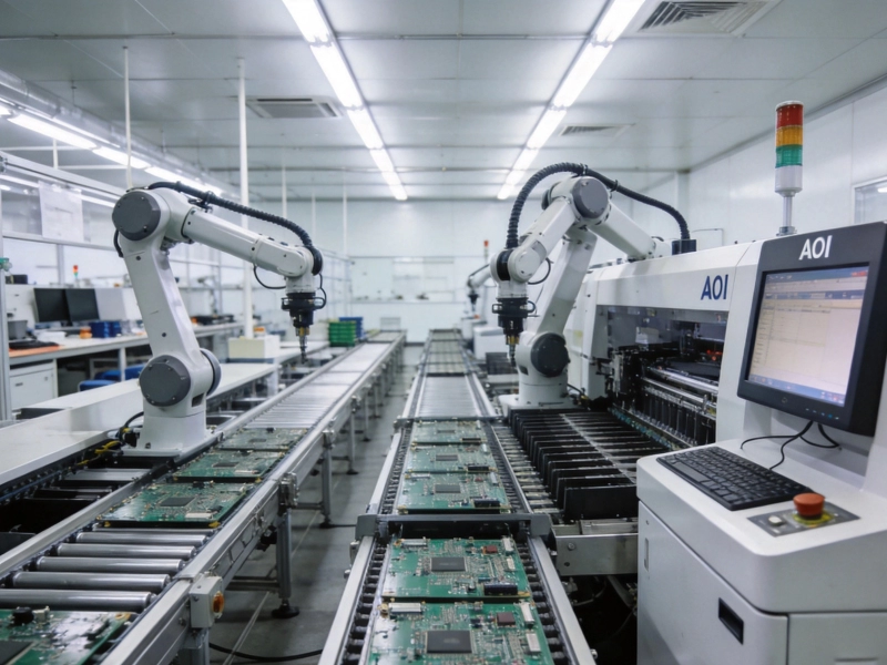
How to Source Reliable Industrial SMT PCB Assembly from Trusted China ManufacturersJuly/29/2026
High Frequency PCB Applications: Designing for Extreme EnvironmentsOctober/13/2026