Open Nav

When RF power reaches hundreds of watts or frequencies climb into GHz ranges, ordinary Pcb Manufacturing falls short. Standard fabrication processes, materials, and design rules work fine for consumer electronics and low-power communication devices. But high power RF applications—radar systems, plasma generators, medical equipment, and industrial heating—push PCB capabilities to extremes that demand specialized manufacturing expertise. Understanding what separates capable high frequency PCB manufacturers from general-purpose shops helps engineers specify appropriate partners for demanding applications.
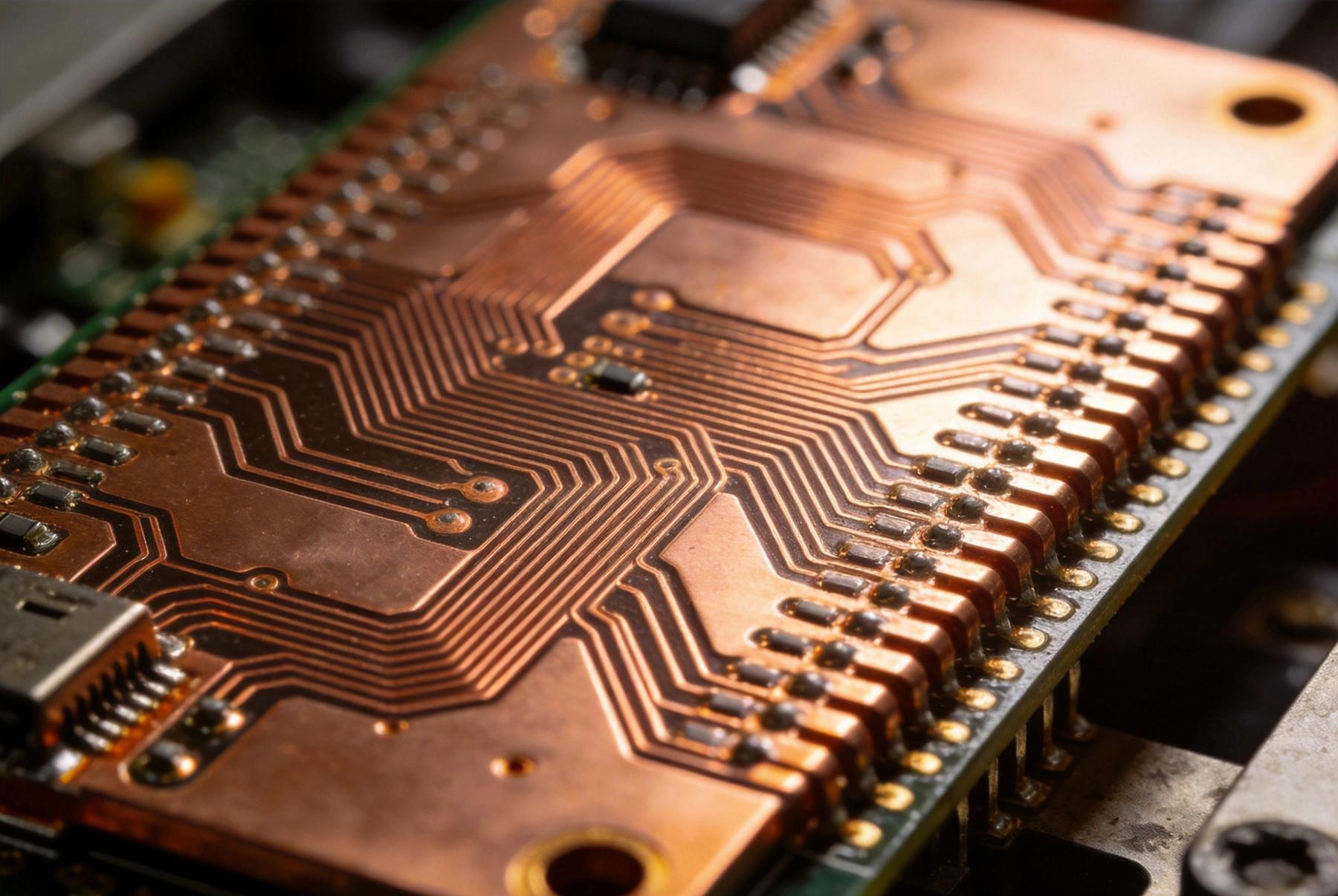
This article examines the manufacturing capabilities, material requirements, and design considerations that enable reliable high power Rf Pcb production. From thick copper handling to thermal management, we explore the technical factors that determine whether a manufacturer can successfully produce boards for demanding RF applications.
RF and high frequency applications share common themes but diverge in their failure mechanisms. High frequency circuits care about Signal Integrity, Impedance Control, and loss characteristics. High power circuits care about thermal management, current capacity, and voltage breakdown. High power RF combines both concerns, requiring designers to balance competing requirements simultaneously.
At high power levels, even small resistive losses generate significant heat. A trace with 0.5 ohm Characteristic Impedance carrying 10A dissipates 50W as heat. This thermal load must go somewhere—through Dielectric Materials, into mounting structures, or dissipated by active cooling. Materials and constructions that work fine at low power become inadequate when thermal loads increase.
Voltage breakdown becomes a concern at high RF power levels. The peak voltage in an RF waveform can exceed the average voltage by factors of two or three. High-Q resonant circuits can develop very high voltages across small components. PCB constructions must provide adequate spacing and dielectric strength to prevent arcing under these conditions.
Standard Fr-4 materials handle low-power applications adequately but degrade under high power conditions. The Glass Transition Temperature (Tg) limits how much thermal stress Fr-4 can withstand before dimensional instability or delamination occurs. High power applications may exceed these limits, requiring specialized materials with higher thermal capability.
Dielectric loss characteristics affect efficiency at high frequencies. Low-loss Materials like Rogers or Panasonic Megtron maintain their loss properties under thermal stress better than standard materials. For high power applications where efficiency translates directly to heat generation, material loss characteristics matter even more than at low power.
Thermal conductivity differences between materials become significant at high power levels. Air is a poor thermal conductor; most PCB dielectrics are not much better. Metal-core substrates, inserts, and thermal vias all contribute to heat spreading that keeps temperatures within acceptable limits.
Standard PCB copper weights range from 0.5 oz to 2 oz per square foot for most applications. High power PCBs routinely use 3 oz, 4 oz, or heavier copper to reduce resistive heating. Some applications require 6 oz, 10 oz, or even thicker copper for extreme current requirements. Each step up in copper weight creates manufacturing challenges that not all shops can address.
Heavy copper Pcb Manufacturing differs from standard production in multiple ways. Etch times increase substantially for thick copper—patterns that take minutes to etch in 1 oz copper may require hours for 4 oz copper. Plating processes must handle thicker deposits without uniformity problems. These processing differences create cost and capability variations between manufacturers.
Trace width design for heavy copper changes proportionally. A 1 oz design with 100-mil trace might become a 400-mil trace at 4 oz if copper thickness scales, or the same width if the application needs maximum conductivity in minimum space. Understanding how copper weight affects design helps specify appropriate manufacturing requirements.
Via plating in heavy copper boards requires special attention. Standard 1 oz plating (25 microns) becomes inadequate for high-current applications; plating must scale with copper weight to maintain current capacity through via barrels. Some manufacturers offer 2 oz, 3 oz, or heavier plating as standard options for power applications.
Uniformity across large panels becomes problematic for heavy copper plating. Edge throw—the difference between plating thickness at panel edges versus centers—increases with plating thickness. Maintaining consistent plating across production panels requires process control that specialized manufacturers provide.
Filling plated through-holes (PTH) to create solid copper vias requires different approaches for heavy copper. Multiple plating passes, followed by fusing, create solid copper barrels suitable for highest-current applications. The process adds cost but provides current capacity far exceeding standard plated vias.
Heavy copper etching requires longer exposure times and careful parameter control. Undercut—lateral etching beneath the resist mask—increases with copper thickness. Maintaining trace width tolerances becomes more challenging; a 10% undercut on 1 oz copper may be acceptable, but the same 10% on 4 oz copper creates significant dimensional deviation.
Pattern plating—plating copper only where traces are needed rather than plating the entire surface then etching—provides better dimensional control for heavy copper designs. This approach deposits copper only in trace and pad locations, reducing material waste and improving feature definition. However, pattern plating requires additional process steps that not all manufacturers support.
Fine-line patterning becomes extremely difficult with very heavy copper. The minimum trace width and spacing achievable at 6 oz copper differs substantially from what is possible at 1 oz. Design rules must account for copper thickness; designs requiring fine features with heavy copper may be physically impossible to manufacture.
RF Transmission Lines must maintain Controlled Impedance while handling high power levels. Microstrip and stripline constructions work similarly to low-power designs, but thermal effects modify behavior. Power-dependent heating changes dielectric properties and trace dimensions, potentially affecting impedance and frequency response.
Conductor-backed structures improve heat spreading for high-power applications. Adding ground planes or heat sink attachments beneath RF traces provides thermal paths that prevent excessive temperature rise. However, these additions change impedance characteristics and must be included in design calculations.
Quarter-wave transformers and Impedance Matching networks handle high power with careful attention to component ratings. Capacitors and inductors must tolerate high RF currents without overheating or failing. At VHF and UHF frequencies, component self-resonance and quality factor (Q) affect power handling capability significantly.
Thermal vias provide heat conduction through the PCB stackup for high-power RF applications. High via density, large via diameters, and copper filling all contribute to thermal performance. The thermal via array should cover the area beneath power components, extending to heat sinking structures at board edges or mounting points.
Metal inserts—copper or aluminum slugs bonded into the PCB stackup—provide superior thermal paths for localized hot spots. These inserts transfer heat directly from component attachment points to mounting surfaces or dedicated heatsinks. The manufacturing process for metal inserts requires specialized capabilities that not all manufacturers provide.
Direct liquid cooling through channels built into the PCB structure represents the extreme end of thermal management. Some manufacturers offer multilayer boards with internal cooling channels that allow fluid flow directly through the PCB. This approach suits the highest-power applications where conventional thermal management proves inadequate.
Rf Circuits require careful attention to ground plane integrity and shielding effectiveness. High-power circuits generate electromagnetic fields that can couple to unintended paths if shielding is inadequate. Multilayer boards with continuous ground planes provide return paths that minimize radiation and coupling.
Via stitching—ground vias placed along signal paths—maintains ground continuity and reduces radiation. High-frequency return currents follow the path of least impedance, which may differ from the physical signal trace. Via stitching keeps return paths close to signal paths, reducing loop area and suppressing radiation.
Shielded enclosures integrated into PCB construction provide additional isolation for sensitive circuits. Cavity resonators, shielded stripline, and coaxial-like structures can be built into multilayer PCBs. These structures require tight manufacturing tolerances but provide isolation impossible with external shielding alone.
Standard Pcb Materials like FR-4 exhibit increasing loss at higher frequencies, but this effect intensifies under thermal stress. High-power RF operation generates heat that raises dielectric loss, creating positive feedback where more loss generates more heat. This cycle can lead to thermal runaway and failure if materials or power levels are not appropriately matched.
Advanced materials like Rogers RT/duroid, TLY, and RO4000 series maintain low loss characteristics under thermal stress. These ceramics-filled hydrocarbon materials provide consistent dielectric properties across temperature ranges that would degrade FR-4 performance. The trade-off is higher material cost and more demanding manufacturing processes.
Thermal conductivity differs significantly between material families. Standard epoxy-glass has thermal conductivity around 0.3 W/mK; some ceramic-filled materials achieve 0.5-0.7 W/mK. For high-power applications where heat spreading matters, material thermal properties significantly influence design success.
Metal-core PCBs with aluminum or copper substrates provide thermal conductivity orders of magnitude better than Dielectric Materials alone. These IMS (Insulated Metal Substrate) constructions place dielectric insulation over metal cores that spread heat efficiently to mounting surfaces or heatsinks.
IMS constructions suit high-power applications but present trade-offs for Rf Design. The metal substrate acts as a lossy ground plane at high frequencies; Controlled Impedance requires careful dielectric thickness control. Some IMS materials are specifically formulated for RF applications, balancing thermal performance with acceptable RF properties.
Direct bonded copper (DBC) substrates—copper-ceramic-copper constructions—provide excellent thermal performance with good RF properties. DBC is common in high-power semiconductor modules but not widely available for PCB-level manufacturing. When DBC-level performance is required, specialized module packaging may be more appropriate than PCB solutions.
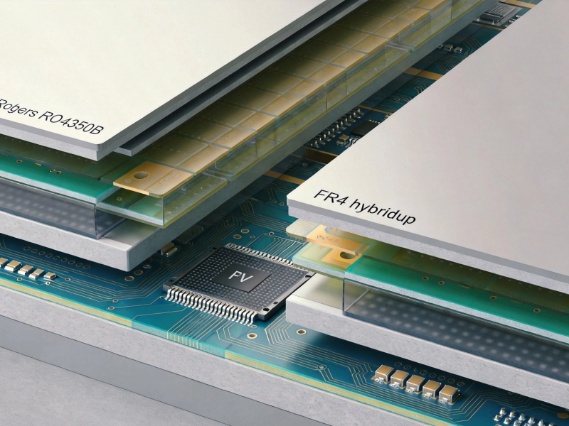
Some applications benefit from combining different materials in hybrid constructions. Rogers material for RF sections can be bonded to standard FR-4 for control circuits, or ceramic-filled materials can interface with metal-core sections. These hybrids require specialized lamination processes and careful thermal expansion matching.
Multilayer constructions with mixed materials present manufacturing complexity. Different materials have different thermal expansion coefficients, creating stress during temperature cycling. Manufacturers experienced with hybrid constructions understand how to manage these mismatches through material selection and process control.
Cost trade-offs between material choices deserve analysis. Premium materials add cost but may enable performance impossible with standard materials. For some applications, expensive materials reduce system cost by eliminating external heatsinks or enabling smaller designs. Total system cost analysis helps justify material investments.
Standard continuity testing verifies connections but doesn't assess power-handling capability. High-power circuits may pass continuity tests yet fail under load due to inadequate trace width, plating thickness, or thermal management. Test requirements should address both electrical connectivity and power handling capability.
Thermal imaging during powered operation identifies hot spots that may indicate manufacturing defects or design limitations. Infrared cameras reveal temperature distribution across boards under realistic operating conditions. This testing catches issues that room-temperature electrical testing misses.
High-potential (hipot) testing verifies dielectric strength under high voltage conditions. Rf Circuits with high-Q resonant structures can develop high voltages even at moderate power levels. Hipot testing ensures that dielectric spacing and material properties provide adequate safety margins.
Cross-section analysis validates internal structure for high-power applications. Via plating thickness, dielectric layer thickness, and copper uniformity all affect performance. Random sampling of production boards through cross-section provides process control data that catches variations before they cause field failures.
3D X-ray Inspection reveals internal structure without destructive sectioning. This non-destructive technique identifies voiding, delamination, and plating uniformity issues throughout production boards. For demanding applications, 100% X-ray Inspection may be warranted despite higher cost.
Surface roughness measurement verifies conductor surface preparation. Rough copper surfaces increase effective resistance at high frequencies, reducing efficiency and increasing heating. The Skin Effect at RF frequencies means current flows primarily near conductor surfaces; surface finish matters even when conductivity through copper cross-section is adequate.
Statistical process control (SPC) ensures consistent quality across production runs. Tracking critical parameters—plating thickness, etch bias, registration—over time reveals trends that might escape inspection of individual boards. Manufacturers with SPC programs provide more consistent results than those reacting to individual board inspections.
Process documentation and certification requirements vary by application. Medical and aerospace applications may require detailed process records, material certifications, and conformance documentation. Understanding what documentation your application requires helps specify appropriate quality systems.
First-article inspection (FAI) validates that new designs can be manufactured to specification. FAI includes dimensional verification, electrical testing, and often cross-section analysis. This qualification step catches design or manufacturing issues before production commitment, reducing risk for both parties.
High-power trace design must account for both DC current capacity and RF effects. IPC current-carrying charts provide DC guidelines, but RF current concentrates near conductor edges due to Skin Effect. Wider traces provide more current-carrying capacity but may suffer from mode issues at very high frequencies.
Temperature rise limits affect trace width calculations. Different applications tolerate different operating temperatures; trace width design must target appropriate temperature rise above ambient for the specific application. Military and aerospace applications typically specify tighter temperature limits than industrial applications.
Spacing between high-power traces and other features must prevent coupling and arcing. High-voltage nodes require creepage and clearance distances appropriate for operating voltage. RF coupling between adjacent traces may cause interference or unwanted mixing products in sensitive receivers.
Via placement affects RF current flow and ground return paths. Inductive vias introduce impedance that may or may not be tolerable depending on circuit function. For critical RF paths, electromagnetic simulation helps optimize via placement before manufacturing.
Thermal via placement for heat spreading should cover the area beneath heat-generating components. Via diameter and spacing affect thermal resistance; optimization balances thermal performance against routing constraints and manufacturing capability. Larger, more closely spaced vias provide better thermal spreading.
Via fencing—rows of vias around sensitive circuits—provides shielding and helps control electromagnetic radiation. Via spacing relative to wavelength determines shielding effectiveness; spacing below one-tenth wavelength provides good isolation for most applications.
Component pad sizing affects both manufacturing reliability and thermal performance. Larger pads improve heat transfer from components to PCB but may increase parasitic capacitance that affects RF performance. Balance between thermal and RF considerations guides optimal pad design.
Solder mask dam requirements differ for heavy copper designs. Minimum mask openings may be specified relative to pad size; very small openings may be impossible to manufacture reliably. Understanding manufacturer capabilities helps specify achievable pad geometries.
Test point sizing and placement affect probe accessibility and contact resistance. High-power circuits may require temperature monitoring or voltage measurement at specific locations; test points should be sized and placed to facilitate this measurement without affecting circuit performance.
Not all manufacturers claiming high-frequency capability can handle thick copper and high power applications. The combination of requirements—RF materials, heavy copper, thermal management features—requires capabilities beyond basic high-frequency or power electronics expertise. Capability verification through audit or sample evaluation helps identify qualified partners.
Requesting examples of previous work in similar applications provides evidence of relevant experience. Manufacturers should be able to share case studies, sample boards, or customer references demonstrating high-power RF capability. Experience with similar applications indicates process knowledge that general-purpose shops lack.
Equipment assessment reveals manufacturing capability limits. Plating line capacity, etching equipment capability, thermal management features, and testing instrumentation all affect what a manufacturer can produce. Asking about specific equipment helps evaluate whether capabilities match requirements.
Rf Material suppliers have approved manufacturer lists indicating which PCB shops can work with specific materials. Using approved manufacturers ensures proper material handling, processing, and quality verification. Material suppliers can often recommend appropriate manufacturers for challenging applications.
Long-term material availability affects product lifecycle planning. Materials may be discontinued or reformulated; manufacturers with strong supplier relationships can often obtain materials for extended periods or identify equivalent replacements. This continuity support matters for products with multi-year lifecycles.
Material certification and traceability provide documentation that some applications require. Material data sheets specify nominal properties, but lot-to-lot variation affects performance. Manufacturers who certify material lots and maintain traceability help applications requiring documented material compliance.
Design for Manufacturability (Dfm) feedback from experienced manufacturers helps optimize designs before production. Manufacturers familiar with high-power RF applications can identify potential manufacturing or reliability issues that designers might miss. Early collaboration reduces costly redesigns and improves first-pass success.
Failure analysis support helps identify root causes when problems emerge during testing or field use. Manufacturers with experienced engineering teams can investigate failures, recommend corrections, and implement process changes that prevent recurrence. This support capability differentiates committed partners from transactional suppliers.
Prototype support options enable design validation before committing to production tooling. Quick-turn prototypes from production-capable manufacturers validate designs under realistic conditions rather than simplified test structures. This validation investment often pays for itself through improved production yields.
Thermal runaway occurs when heating increases loss, which increases heating further. The cycle continues until components fail or derate permanently. Preventing thermal runaway requires understanding material behavior under stress and designing for adequate thermal margins.
Hot spots develop where local heating exceeds surrounding areas. These may result from concentrated current, poor thermal spreading, or material defects. Thermal simulation during design identifies potential hot spots before manufacturing; thermal imaging during testing validates thermal behavior.
Active cooling, improved thermal spreading, and power reduction all address thermal challenges. The appropriate solution depends on application constraints—some designs can add heatsinks; others must operate without active cooling. Understanding thermal requirements drives design decisions.
Delamination—the separation of layers within the PCB—causes failures that may not be immediately apparent. Thermal cycling, moisture absorption, and thermal expansion mismatch all contribute to delamination risk. High-power operation accelerates these mechanisms through thermal stress.
Material compatibility between dielectric layers and metal conductors affects long-term reliability. Different thermal expansion coefficients create stress during temperature cycling. Well-designed constructions account for these mismatches through material selection, layer ordering, and thermal management.
Manufacturing process control prevents delamination that results from process defects. Incomplete cure, contamination, and improper lamination parameters all create conditions for later delamination. Quality manufacturers control these factors to prevent process-induced failures.
High voltage nodes in RF circuits risk arcing through air or along PCB surfaces. Surface contamination, humidity, and dust all reduce breakdown voltage. Clean manufacturing, conformal coating, and adequate spacing prevent arcing failures.
Partial discharge—small ionization events that erode insulation over time—causes latent failures in high-voltage applications. Materials and constructions rated for the voltages present in high-power RF circuits should be specified based on application requirements and safety margins.
Creepage and clearance distances specified by safety standards address voltage breakdown concerns. These requirements vary by application—medical, aerospace, and industrial applications may have different standards. Understanding applicable standards ensures appropriate design for the specific use environment.
Silicon Carbide (SiC) and Gallium Nitride (GaN) semiconductors enable higher power densities than silicon, pushing PCB thermal requirements higher still. The switching speeds of these devices also increase Electromagnetic Interference concerns. PCB technology must evolve to support the thermal and RF challenges these devices create.
Integrated power modules combine semiconductor devices with optimized thermal management and RF interfacing. These modules may use DBC substrates, direct liquid cooling, and integrated passives that push PCB-level technology further than discrete component approaches can achieve.
New dielectric materials with improved thermal conductivity and lower loss continue to emerge. Graphite-based substrates, nano-filled dielectrics, and engineered ceramics offer performance improvements that standard materials cannot match. Staying current with material development enables access to improved capabilities.
Manufacturing processes continue advancing, enabling finer features and better thermal management. Additive manufacturing techniques, advanced plating methods, and improved metrology all contribute to expanded capability. Partners investing in process development provide access to these improvements.
The trend toward system-level integration affects PCB requirements. More functionality integrated into single modules reduces board count but increases complexity of individual boards. High power RF functions may coexist with sensitive receivers on boards requiring careful isolation design.
3D integration—stacking boards or embedding components—provides density improvements beyond what planar PCB technology can achieve. These approaches combine PCB technology with packaging techniques, requiring collaboration across traditional boundaries.
Copper weight depends on current, frequency, and acceptable temperature rise. As a general guideline, 2-4 oz copper handles moderate RF power (tens of watts); 4-6 oz suits higher power; extreme applications may require 10 oz or heavier. Exact requirements should be calculated based on specific application parameters and validated through thermal analysis or testing.
Standard FR-4 may work for low to moderate RF power with adequate thermal management. However, FR-4 exhibits higher loss at high frequencies and lower thermal capability than specialty materials. For demanding applications with significant power levels, Low-loss Materials like Rogers or ceramic-filled substrates provide better reliability and efficiency.
Essential thermal features include thermal vias beneath heat-generating components, metal backing or inserts for heat spreading, and adequate spacing for convection or forced-air cooling. Component selection should consider thermal resistance from junction to case. For extreme applications, liquid cooling channels or direct bonding to heatsinks may be necessary.
Request examples of previous work in similar applications, verify material relationships with Rf Material suppliers, and consider first-article inspection of prototypes. On-site audits allow direct assessment of equipment and process controls. Previous customer references provide additional validation of capability claims.
Recommended testing includes electrical continuity, hipot testing for dielectric strength, thermal imaging under powered operation, and potentially X-ray inspection for internal quality. Cross-section analysis validates internal structure. The specific test program depends on application requirements and criticality.
High power Rf Pcb Manufacturing demands capabilities that go beyond standard PCB shops. The combination of thick copper handling, RF materials, thermal management, and quality control creates requirements that specialized manufacturers address through equipment, process knowledge, and experience. Understanding these requirements helps engineers specify appropriate manufacturing partners and design for successful production.
The technical factors explored here—copper weight capability, plating quality, material selection, thermal management, and testing—combine to determine whether a manufacturer can reliably produce boards for demanding applications. No single capability compensates for weaknesses in others; balanced capability across all requirements enables successful high power Rf Pcb production.
As RF power levels continue increasing and frequencies push higher, the manufacturing challenges grow correspondingly. Manufacturers investing in advanced capabilities position themselves to serve applications that less-equipped competitors cannot address. For engineers working on demanding RF systems, identifying and qualifying these capable partners becomes increasingly important.
The convergence of thermal management, RF performance, and manufacturing capability defines the envelope of what is achievable in high power Rf Pcb Design. Within this envelope, successful products balance performance, cost, and reliability to meet application requirements. Understanding the technical foundations covered here provides the basis for making those tradeoffs effectively.

High Frequency PCB Capabilities for Aerospace and Defense ApplicationsJuly/17/2026

Our Latest High Frequency PCB Capabilities for 6G ResearchMay/29/2026

How Our High Frequency PCB Capabilities Support High-Speed Data CentersAugust/08/2026
Understanding High Frequency PCB Capabilities: Line Width, Spacing, and Layer CountJune/28/2026

Why Advanced Testing Equipment Defines Top High Frequency PCB CapabilitiesJuly/07/2026
The Importance of Impedance Control in Our High Frequency PCB CapabilitiesSeptember/03/2026
Pushing the Limits: Our Latest High Frequency PCB Capabilities for 6G ResearchJune/11/2026
Exploring Our High Frequency PCB Capabilities in Mixed Material LaminationJuly/29/2026