Open Nav

In the realm of high frequency printed circuit boards, where signals travel at speeds approaching the speed of light and wavelengths shrink to millimeters, Impedance Control represents the fundamental difference between circuits that function reliably and those that fail mysteriously. Our high frequency PCB capabilities center fundamentally on our ability to manufacture boards with precise, consistent impedance characteristics across a wide range of frequencies from megahertz to millimeter-wave. This capability enables our customers to design circuits that transmit signals with minimal distortion, maximum power transfer, and predictable performance. Understanding why Impedance Control matters so critically in high frequency applications helps engineers appreciate the technical depth required for successful RF and microwave Pcb Manufacturing. This comprehensive exploration explains the principles, practices, and capabilities that enable superior impedance control in our high frequency PCB manufacturing processes.
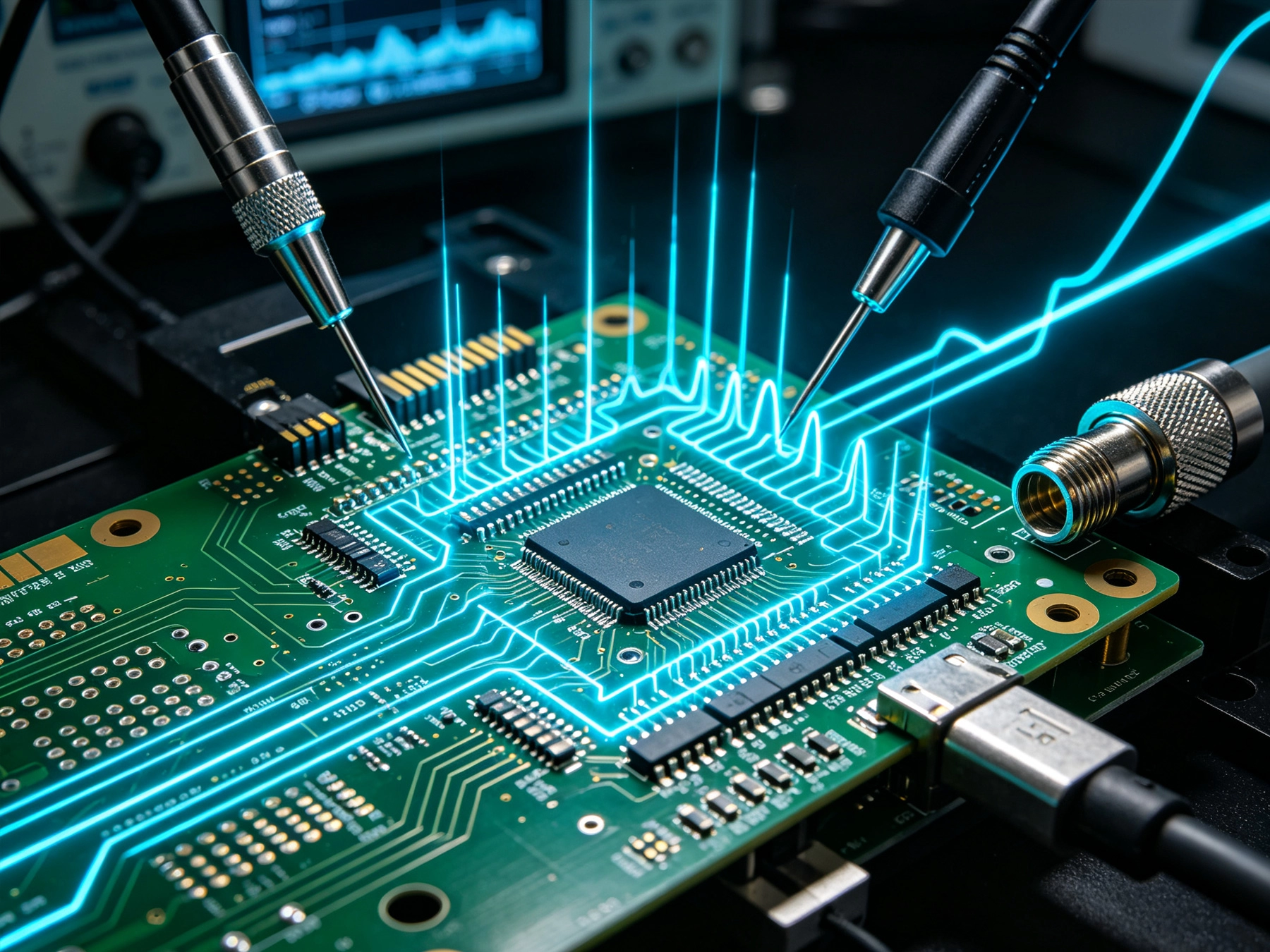
Impedance represents the opposition that a circuit presents to alternating current flow, combining resistance with reactance from capacitance and inductance. At low frequencies, impedance effects are minimal and traditional PCB design practices suffice. However, as frequencies rise into the RF and microwave spectrum, impedance becomes the dominant factor determining circuit behavior. Signal propagation on Transmission Lines exhibits wave-like behavior where Characteristic Impedance—the impedance a Transmission Line would present if infinitely long—determines how signals travel without reflection. Mismatches between source impedance, line impedance, and load impedance cause signal reflections that travel back and forth along transmission paths, distorting signal waveforms and wasting power. The Skin Effect at high frequencies causes current to flow primarily on conductor surfaces, increasing effective resistance and making impedance more sensitive to conductor geometry. Dielectric losses increase with frequency, adding to signal attenuation and making material selection critical for high frequency performance. Understanding these high frequency phenomena provides the foundation for appreciating why precise impedance control matters so fundamentally in RF and Microwave Pcb design and manufacturing.
Signal Integrity represents the primary concern driving impedance control requirements in high frequency circuits. When impedance varies from design specifications, signal waveforms distort, creating timing errors, reduced noise margins, and potential data corruption in digital applications. Reflection coefficients quantify the fraction of signal power reflected at impedance discontinuities, with even small discontinuities causing measurable signal degradation at high frequencies. Standing waves form when reflections from multiple discontinuities combine, creating voltage and current variations along Transmission Lines that stress components and reduce efficiency. Return loss—a measure of reflected signal power—directly impacts system performance, with poor return loss reducing available signal power and increasing noise floor. Insertion Loss from impedance mismatch compounds with conductor and dielectric losses, reducing Power Delivery to loads and limiting system range in wireless applications. Phase distortion from frequency-dependent impedance characteristics degrades pulse shape fidelity in digital systems and introduces errors in phase-modulated communication signals. The cumulative effect of impedance variations across a system budget determines whether a design functions reliably or exhibits intermittent failures that prove extremely difficult to diagnose and fix.
Achieving precise impedance control requires manufacturing processes held to extremely tight tolerances across multiple parameters. Trace width control directly impacts impedance for Microstrip and stripline structures, with tolerances of ±0.5 mils or better often required for 1-2% impedance tolerance. Dielectric thickness control determines spacing between conductors and reference planes, with similar tight tolerances required for consistent impedance. Dielectric Constant variation in substrate materials—typically ±2-5% for standard materials—directly translates to impedance variation, making material selection and lot control critical. Copper roughness affects effective Dielectric Constant and losses at high frequencies, requiring specification and control of conductor surface finish. Etch factor—the ratio of trace width at base versus top—influences effective geometry and impedance, particularly for fine-line features. Plating thickness uniformity affects Ground Plane spacing and conductor geometry in plated-through structures. Lamination parameters influence dielectric thickness and resin content in multilayer constructions. Our manufacturing processes implement statistical process control across all critical parameters, maintaining Cpk values exceeding 1.33 for impedance-critical characteristics and verifying impedance on 100% of Controlled Impedance boards using time-domain reflectometry and vector network analysis.
Material selection fundamentally determines achievable impedance control and high frequency performance. Standard Fr-4 materials exhibit dielectric loss tangents that cause significant signal attenuation at frequencies above approximately 5 GHz, making them unsuitable for high frequency applications. High-frequency laminates including Rogers, Taconic, and Isola materials offer lower loss tangents and more stable dielectric constants across frequency and temperature. Dielectric constant consistency across material batches directly impacts impedance consistency, with tighter material tolerances enabling tighter impedance control. Ceramic-filled Ptfe materials provide excellent electrical properties with good dimensional stability, though at higher cost than conventional materials. Hydrocarbon ceramic materials offer a cost-effective middle ground with good high frequency performance and better processability than pure Ptfe. Reinforcement type influences dielectric constant uniformity, with spread glass weaves providing more consistent properties than conventional woven glass. Material data sheet values represent typical values, but actual dielectric constants vary from lot to lot, requiring verification testing for the most demanding applications. Our material qualification process verifies dielectric constant and loss tangent for each incoming lot, maintaining material traceability and ensuring consistent electrical performance across production runs.
Successful Controlled Impedance designs require collaboration between designers and manufacturers from project inception. Design rule definition based on manufacturer capabilities ensures specified tolerances fall within achievable ranges rather than demanding impossible precision. Stackup design for multilayer impedance-controlled boards requires careful consideration of layer sequencing, plane placement, and prepreg specifications. Reference plane continuity in the areas surrounding controlled impedance traces is essential for maintaining predictable impedance, requiring careful attention to plane routing and split plane placement. Via placement near controlled impedance traces creates discontinuities that must be accounted for in design or avoided through careful routing. Test coupon design enables verification of impedance performance across panels, providing correlation between simulation and actual manufacturing results. Trace spacing from adjacent features affects coupling and effective dielectric environment, influencing impedance in coupled structures. Panel utilization affects manufacturing consistency, with edge effects causing impedance variations near panel edges that must be considered in design. Our engineering support team collaborates with customers during design phase to optimize stackup designs, validate achievable tolerances, and ensure manufacturability of complex impedance requirements.
Verification of impedance control requires sophisticated measurement capabilities beyond simple continuity testing. Time-domain reflectometry (Tdr) measures impedance discontinuities by launching fast rise-time pulses and analyzing reflected signals, providing spatial resolution of impedance variations along transmission paths. Vector network analysis (Vna) characterizes S-parameters including Insertion Loss, return loss, and impedance across frequency ranges, enabling comprehensive electrical performance verification. Differential Impedance Measurement for coupled structures requires Vna configurations that excite and measure differential modes separately. Calibration standards and techniques directly impact measurement accuracy, requiring rigorous calibration procedures and regular verification of calibration artifacts. Test coupon design influences measurement accuracy, with coupon geometry and launch structures requiring careful design to minimize measurement artifacts. Fixture de-embedding techniques remove connector and cable effects from measurements, isolating PCB performance. Statistical analysis of measurement results across panels and lots provides data for process capability assessment and continuous improvement. Our measurement laboratory maintains calibrated Tdr and VNA equipment with traceable calibration to national standards, providing documented verification of impedance performance for each production lot of controlled impedance boards.
Multiple application categories demand precise impedance control for successful operation. 5G communication systems operate at frequencies up to 86 GHz, requiring controlled impedance for RF front-end circuits, filters, and antennas. Radar systems including Automotive Radar at 77 GHz and industrial radar across various frequency bands require precise impedance for transmitter and receiver chains. Satellite Communications depend on controlled impedance for upconverters, downconverters, and feed networks. Test and measurement equipment including spectrum analyzers and network analyzers require impedance control for frequency conversion and signal routing. Military and aerospace systems operating in X-band, Ku-band, and Ka-band demand tight impedance tolerances for phased array antennas and electronic warfare systems. High-speed digital applications including 100 Gbps and 400 Gbps Ethernet require controlled impedance for Serializer-Deserializer (SerDes) channels. Medical Imaging equipment including MRI systems and ultrasound transducers benefit from controlled impedance for signal transmission. Each application category has specific impedance tolerances—typically ranging from ±5% for consumer applications to ±2% for industrial and ±1% for aerospace and defense—determining manufacturing complexity and cost.
Our high frequency pcb manufacturing capabilities encompass equipment and processes specifically designed for controlled impedance applications. Imaging systems using direct laser exposure provide resolution and accuracy exceeding photographic processes, enabling precise trace geometry control. Plasma desmear and activation processes prepare hole walls for consistent plating while maintaining controlled dielectric properties. Sequential lamination with precise pressure and temperature control ensures uniform dielectric thickness across panels and lots. Rf Testing capabilities including TDR and VNA systems with frequency coverage to 67 GHz enable comprehensive impedance characterization. Material handling and storage procedures minimize contamination and moisture absorption that could affect electrical properties. Environmental controls maintain temperature and humidity within tight ranges during critical processing steps. Statistical process control systems monitor critical parameters in real-time, triggering alerts for out-of-control conditions. Our capability profile includes impedance tolerances as tight as ±2% for single-ended structures and ±3% for differential pairs across frequencies from DC to 67 GHz, with special processes available for tighter tolerances in critical applications.
Quality Assurance for controlled impedance boards extends beyond standard PCB inspection to encompass comprehensive electrical verification and documentation. Impedance testing of production coupons verifies process capability for each panel, with data recorded for traceability. Certificate of conformance documents impedance test results for each production lot, providing customers with documented verification of specifications. Material certifications include dielectric constant and loss tangent data for each material lot used in production. Process capability documentation quantifies Cpk values for impedance-critical parameters, enabling informed decisions about design tolerance specification. First article inspection for new designs includes comprehensive electrical testing and documentation before production approval. Failure analysis capabilities investigate impedance-related failures, identifying root causes and implementing corrective actions. Continuous improvement programs analyze impedance data across production runs, identifying opportunities for process optimization. Our Quality Management System maintains complete traceability from incoming materials through final inspection, enabling rapid investigation and resolution of any quality concerns.
Controlled impedance manufacturing inevitably costs more than standard PCB production, with cost scaling with required precision and frequency range. Tighter impedance tolerances demand more precise processes, more intensive inspection, and higher material specifications, all adding to cost. Higher frequency materials cost more than standard substrates, with advanced materials commanding significant price premiums. Test-intensive verification including 100% impedance testing adds to production costs compared to statistical sampling approaches. Panel utilization affects cost, with impedance-controlled areas requiring space for test coupons and process control features. Lot size economics favor larger production volumes, spreading fixed costs across more boards. Cost optimization involves specifying tolerances no tighter than actually required by application—±10% tolerance costs significantly less than ±5%, which costs less than ±2%. Working with manufacturers during design phase can identify cost-effective stackup solutions that meet requirements without excessive precision. The cost premium for controlled impedance should be evaluated against the cost of Signal Integrity failures, field returns, and project delays that can result from inadequate impedance control.
high frequency pcb requirements continue evolving toward higher frequencies, tighter tolerances, and more complex structures. 5G mmWave rollout is driving demand for boards operating at 28 GHz, 39 GHz, and 86 GHz, requiring impedance control at unprecedented frequencies. Automotive Radar at 77 GHz and above demands tight tolerances for safety-critical systems where signal integrity directly impacts system reliability. 6g Research is already exploring frequencies above 100 GHz, pushing manufacturing capabilities toward new limits. Advanced packaging including embedded active devices and chip-scale packaging creates impedance challenges at component level. Integrated photonics and RF-photonics circuits blend optical and electrical transmission, requiring impedance control at both electrical and optical interfaces. Additive manufacturing techniques may eventually enable manufacturing approaches impossible with subtractive processes. Our continuous investment in equipment, process development, and engineering expertise ensures we remain at the forefront of High Frequency Pcb Capabilities, ready to meet evolving customer requirements.
Impedance control represents the cornerstone of high frequency Pcb Manufacturing capability, enabling reliable signal transmission in applications from 5G communications to automotive radar to high-speed data links. Our comprehensive approach to impedance control encompasses material selection and qualification, stackup design optimization, precise manufacturing process control, sophisticated measurement and verification, and comprehensive documentation. This end-to-end capability ensures that boards we produce meet impedance specifications that enable our customers to achieve their performance objectives. As high frequency applications continue proliferating across communications, automotive, aerospace, medical, and industrial sectors, demand for precise impedance control will only increase. Our commitment to maintaining and advancing our impedance control capabilities positions us to serve our customers' current needs while preparing for future requirements. The combination of engineering expertise, manufacturing capability, quality systems, and collaborative customer relationships creates the foundation for successful High Frequency Pcb manufacturing that our customers depend on for their most demanding applications.
What impedance tolerances can you achieve?
We typically achieve ±5% impedance tolerance for standard controlled impedance applications, ±2-3% for precision applications, and ±1% for the most demanding applications requiring specialized processes. Differential impedance tolerances are typically ±3-5% for standard and ±2-3% for precision. The achievable tolerance depends on frequency range, board complexity, stackup design, and material selection. Our engineering team can advise on achievable tolerances for specific requirements.
What frequency range do your impedance control capabilities cover?
Our impedance control capabilities extend from DC through 67 GHz using vector network analysis verification. This frequency range covers applications including 5G sub-6 GHz and mmWave, automotive radar at 24 GHz and 77 GHz, Satellite Communications, wireless infrastructure, and high-speed digital to 100+ Gbps. Special processes can address requirements extending to higher frequencies for research and development applications.
How do you verify impedance control on production boards?
We verify impedance control through multiple methods: time-domain reflectometry (TDR) measures impedance discontinuities and average impedance along transmission paths, vector network analysis (VNA) characterizes S-parameters including insertion loss and return loss across frequency ranges, test coupons on each panel provide process verification and correlation data, and statistical analysis of measurement results documents process capability. All impedance-critical boards receive 100% testing with results documented in certificates of conformance.
What materials do you use for high frequency applications?
We stock a comprehensive range of high-frequency materials including Rogers RT/duroid, Rogers RO4000 series, Taconic RF substrates, Isola I-Speed and I-Ceres, and various hydrocarbon ceramic materials. Material selection depends on frequency range, loss requirements, thermal performance, and cost considerations. Our engineering team can recommend optimal materials for specific applications and frequency ranges.
How does impedance control affect production lead time and cost?
Controlled impedance boards typically require 1-2 additional days compared to standard boards for impedance testing and documentation. Cost premiums range from 20-40% for standard controlled impedance (±5% tolerance) to 50-100% for precision impedance (±2% tolerance) with specialized materials. The premium reflects tighter process control, enhanced inspection, specialized materials, and documentation requirements. Working with us during design phase can optimize designs for cost-effective manufacturing while meeting performance requirements.

How Our High Frequency PCB Capabilities Support High-Speed Data CentersAugust/08/2026

Our Latest High Frequency PCB Capabilities for 6G ResearchMay/29/2026
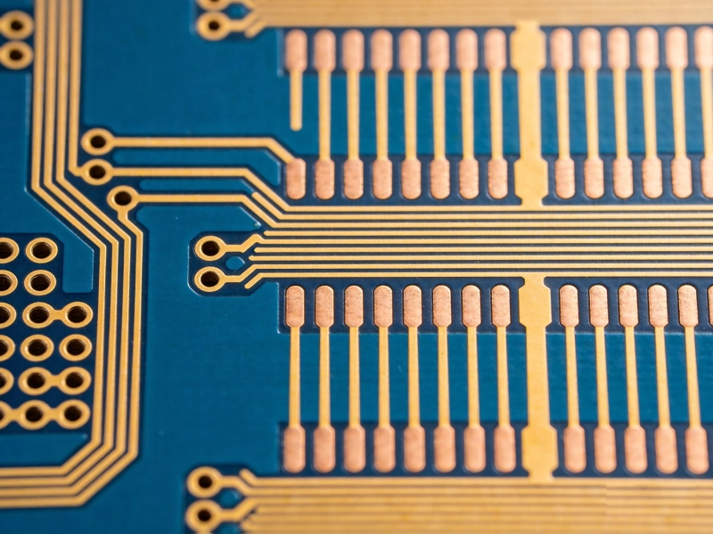
Understanding High Frequency PCB Capabilities: Line Width, Spacing, and Layer CountJune/28/2026
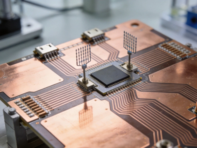
A Deep Dive into High Frequency PCB Capabilities for Millimeter Wave TechSeptember/24/2026
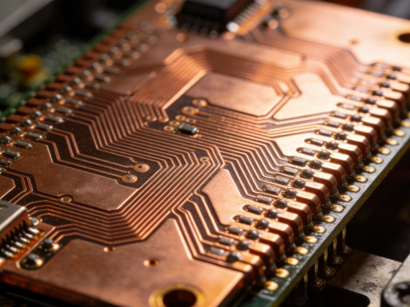
High Frequency PCB Capabilities: Handling Thick Copper and High Power RFSeptember/15/2026
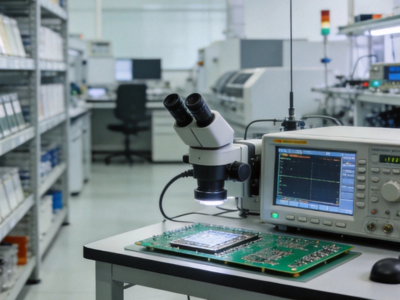
Upgrading Your Supply Chain with Our Expanded High Frequency PCB CapabilitiesOctober/09/2026

Why Advanced Testing Equipment Defines Top High Frequency PCB CapabilitiesJuly/07/2026
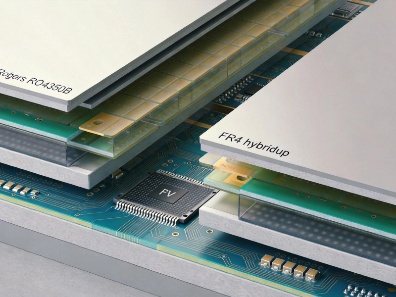
Exploring Our High Frequency PCB Capabilities in Mixed Material LaminationJuly/29/2026