Open Nav
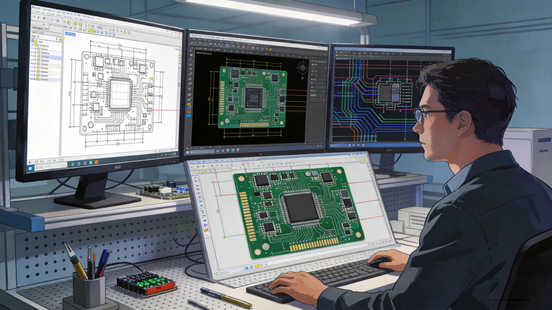
So you're a hardware engineer looking to level up your High Frequency Pcb skills? You're in the right place. Whether you're transitioning from digital designs to RF work, or just want to fill gaps in your knowledge, this guide covers the essential stuff you gotta understand to design PCBs that actually work at high frequencies.
The thing about high frequency design is - it ain't just regular PCB design with faster signals. At frequency, the physics changes. Your traces stop acting like simple wires and start behaving like transmission lines. Your ground planes become critical infrastructure. Your Component Placement decisions matter in ways that don't exist at lower frequencies. Get these fundamentals wrong and your designs will fail in ways that's really hard to debug. Get them right and you're equipped to tackle everything from WiFi modules to 5G front-ends.
At low frequencies, you can think of PCB traces as simple connections. Current flows from point A to point B, resistance determines voltage drop, and everything follows Ohm's law nicely. This mental model works fine when signals change slowly - like a 1 MHz microcontroller toggling an IO pin.
But when signals start toggling faster - let's say edges in the nanosecond range - the story changes. Those fast edges contain high frequency harmonics even if the fundamental clock rate seems modest. And at these frequencies, your trace starts behaving like a transmission line. Instead of just connecting two points, it becomes a structure that guides electromagnetic waves.
What changes at high frequency:
Understanding this transition is the foundation for everything else. Once you get that your PCB traces are actually transmission lines, the rest of high frequency design starts making sense.
Not every PCB needs RF-level attention. Here's how to know when you need to shift your thinking:
Rules of thumb for high frequency consideration:
If you're designing a simple 1 MHz microcontroller board with 10cm traces, you can largely ignore transmission line effects. But if you're doing anything with wireless, high speed data, or fast edges, you need to apply what we're covering here.
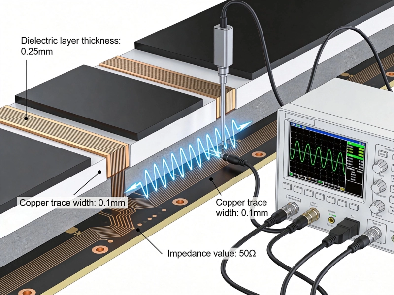
Every transmission line structure has a Characteristic Impedance (Z0) - the ratio of voltage to current for a wave propagating along the line. For PCB traces over ground planes, this impedance depends on trace geometry and the PCB material properties. The standard target is 50Ω for single-ended signals and 100Ω differential.
Impedance depends on:
PCB design tools calculate impedance based on these parameters. The tricky part is that fabrication tolerances mean your actual impedance will vary from design values. Trace width might be ±10%, substrate thickness might vary ±10%, material Dk might vary ±5%. These variations stack up, so understanding what tolerance you can achieve matters for Controlled Impedance design.
You might wonder why 50Ω became the standard. It wasn't arbitrary - there are practical reasons. 50Ω represents a balance between power handling, Signal Loss, and physical size that works well for most applications.
Why 50Ω became standard:
100Ω differential came later for differential signaling standards. The differential impedance is twice the single-ended impedance for well-coupled pairs, or about 100Ω for most differential designs.
Two basic transmission line structures are used in PCBs:
Microstrip: Trace on the outer layer with ground plane beneath. Signal propagates partly in air and partly in dielectric. Easier to fabricate and access for measurement. Higher loss than stripline but simpler.
Stripline: Trace embedded between two ground planes. Signal propagates entirely in dielectric. Better shielding and lower radiation, but harder to fabricate and test. Lower loss at very high frequencies.
When to use each:
For most hardware engineers working on everything from WiFi to cellular to high speed digital, microstrip is the starting point. Stripline comes into play when you need better isolation or are working at frequencies where microstrip radiation becomes problematic.
Modern PCB design tools calculate trace dimensions for target impedance automatically. But understanding the calculation helps you make good design decisions and troubleshoot when things don't work as expected.
Key calculations:
Online calculators and design tool features let you find trace dimensions for target impedance. The workflow is typically: decide target impedance (50Ω, 100Ω differential, etc.), select substrate material, then calculate trace width needed.
Practical design workflow:
The fabricator step is critical. Give them your stack-up and impedance requirements, and ask what tolerance they can achieve. Standard fabrication typically gives ±10% impedance tolerance. Tighter tolerances cost more but might be necessary for sensitive applications.
Many high speed interfaces use differential signaling - USB, PCIe, HDMI, Ethernet, etc. Differential pairs have specific design requirements beyond single-ended transmission lines.
Differential pair fundamentals:
Length matching guidelines:
The specific matching requirement depends on your interface specification and data rate. Higher speeds need tighter matching. Check your interface specification for exact requirements.
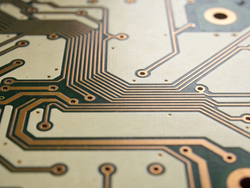
Vias - the holes connecting layers - create impedance discontinuities. At high frequency, via effects become significant enough to affect signal quality. Understanding via design helps you minimize these effects.
Via effects on signals:
Minimizing via effects:
For most designs, a few vias on high speed signals won't cause problems. But for very high frequencies or sensitive applications, via design becomes more critical. When in doubt, simulate or test with your fabricator.
The PCB substrate material affects high frequency performance significantly. Different materials have different dielectric properties, thermal characteristics, and costs. Choosing the right material for your application is a fundamental design decision.
Key material properties:
Dk affects impedance calculation - higher Dk gives lower impedance for the same geometry. Df affects signal loss - higher Df means more loss, especially important at high frequencies.
Standard FR4 works for many applications but has limitations at higher frequencies. Understanding when FR4 is adequate versus when you need specialized materials helps you make cost-effective design decisions.
FR4 characteristics:
When FR4 works:
When you need better materials:
When FR4 won't work, you have several material options. Each has trade-offs between performance, cost, and fabrication practicality.
Rogers RO4000 series:
Rogers RO3000 series:
Other options:
Your fabricator's experience matters as much as material specifications. A fabricator experienced with RO4000 will probably give better results than one trying RO3000 for the first time. Match material to fabrication capability.
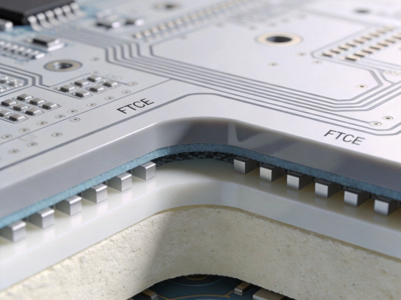
The PCB stack-up - the arrangement of copper layers, Dielectric Materials, and prepreg - fundamentally affects high frequency performance. Good stack-up design provides controlled impedance, adequate ground reference, and practical fabrication.
Basic stack-up principles:
Typical 4-layer stack-up for high frequency:
Typical 6-layer stack-up:
More layers give more flexibility for signal routing and ground plane continuity. For complex high frequency designs, 6-8 layers is common.
Ground planes are critical infrastructure in high frequency PCBs. They provide reference for impedance, return current path, and shielding. Poor ground plane design causes many high frequency problems.
Ground plane principles:
What not to do:
Think of ground planes as the highway for return current. Any interruption forces traffic to find alternate routes, creating inductance and potential EMI issues.
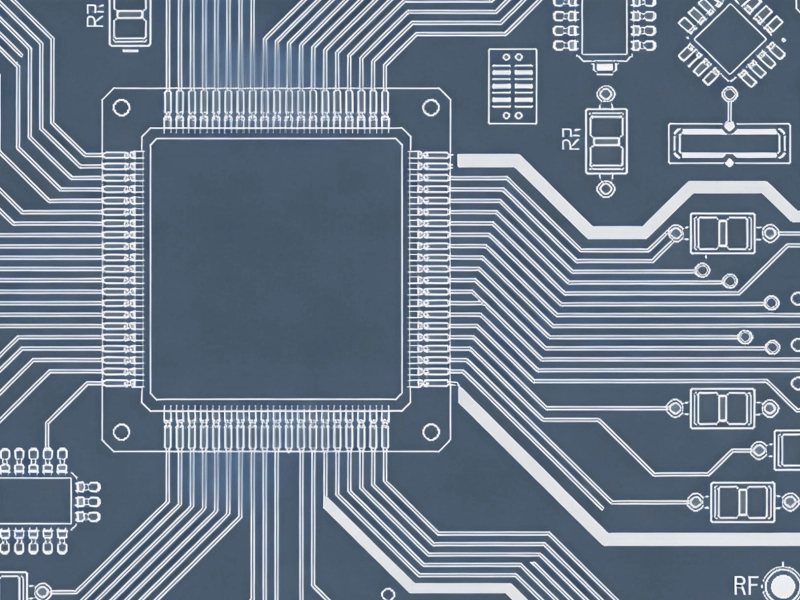
Component Placement affects high frequency performance significantly. Thinking about placement from a Signal Integrity perspective helps avoid problems later.
Placement considerations:
RF component placement:
How you route traces affects signal quality. These guidelines help you avoid common problems:
Impedance controlled routing:
Differential pair routing:
Crosstalk control:
Every signal current needs a return path. At high frequency, the return current doesn't flow through whatever path seems convenient - it follows the signal trace on the reference plane, directly beneath it. Understanding this behavior is essential for good high frequency design.
High frequency return current behavior:
The key insight: if you put a gap in your ground plane under a high frequency signal trace, the return current has to go around the gap, creating a loop that radiates and causes EMI problems. Keep ground planes continuous under your high frequency signals.
EMI (electromagnetic interference) can cause your board to interfere with other devices or be interfered with itself. Good high frequency design practices minimize EMI.
Emi Reduction techniques:
Common EMI mistakes:
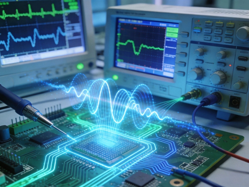
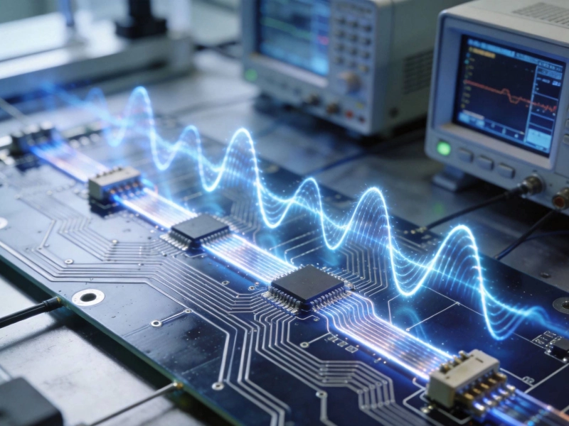
You can't just trust that your design will work - you need to test. Understanding basic high frequency testing helps you validate your designs and troubleshoot problems.
Essential test equipment:
Key measurements:
Test coupons - specialized transmission line structures on your PCB - let you verify fabrication achieved target impedance without measuring actual circuit traces. Every controlled impedance board should include test coupons.
Test coupon design:
Request impedance test data from your fabricator. Compare their measured results against design targets. If there's significant discrepancy, you may need to adjust design for your specific fabricator's process.
These are the mistakes we see most often when engineers transition to high frequency design:
1. Ignoring transmission line effects
"It's just a short trace, it won't matter." Wrong. Even a few centimeters of trace at high frequency behaves as a transmission line. Always use controlled impedance for high frequency signals, regardless of length.
2. Treating all grounds as equal
"Ground is ground." At high frequency, the location of ground connection matters. Current flows in loops, and the return path impedance affects circuit behavior. Think about where return current flows.
3. Neglecting fabricator capabilities
"The design tool says 0.25mm trace width." That might not be achievable with good tolerance by your fabricator. Always verify with your specific fabricator before finalizing design.
4. Over-specifying material requirements
"We need the absolute lowest loss material available." Maybe you do, but often FR4 or a moderate-cost material works fine. Over-specifying increases cost without benefit. Match material to actual requirements.
5. Forgetting about tolerance stacking
"My calculation gives exactly 50Ω." But trace width tolerance, substrate thickness tolerance, and material Dk tolerance all stack up. Design with margin for variation, or specify tight fabrication tolerance if needed.
6. Underestimating via effects
"Just add a few vias for grounding." Vias on high frequency signals create discontinuities. Sometimes they're unavoidable, but minimize them on critical paths and consider their effects.
Developing High Frequency Pcb expertise takes time and practice. Here are ways to build your skills:
Study resources:
Practical experience:
Tools to master:
Your fabricator is a crucial partner in high frequency PCB success. Building that relationship helps you get better results.
Questions to ask your fabricator:
Share information:
A good fabricator relationship means you get boards that work, they get clear requirements, and both sides learn over time.
High Frequency Pcb Design is a valuable skill that opens doors to RF, wireless, and high speed digital applications. The fundamentals we've covered - transmission lines, impedance, materials, layout, and testing - provide a foundation for building expertise.
If you're working on a high frequency PCB project and need support, our technical team can help. We have experience across telecommunications, wireless, and high speed digital applications, and we work with hardware engineers to develop PCBs that meet their performance requirements.
Contact us to discuss your project: We'll help you navigate design decisions, material selection, and fabrication requirements for your specific application.
High Frequency Pcb Design is different from low frequency work, but it's learnable. The key is understanding why frequency changes things - how transmission line behavior, Impedance Control, and proper return paths affect your designs. Once you grasp these fundamentals, you can design PCBs that work reliably at frequency.
The essential knowledge we've covered - understanding when frequency matters, transmission line fundamentals, impedance design, material selection, layout guidelines, and testing approaches - gives you what you need to start designing high frequency PCBs with confidence. You'll make mistakes as you learn, but those mistakes teach you more than any article can.
Hardware engineering is about making things work in the real world. High frequency PCB design adds some complexity, but it's complexity you can manage with good fundamentals and practical experience. Start with straightforward projects, test your designs, learn from results, and gradually take on more challenging applications. That's how you build real expertise.
The RF and high speed digital world needs hardware engineers who understand high frequency PCB design. Your career benefits from developing these skills. And honestly, once you get it, there's something satisfying about designing circuits that work at frequencies where the physics gets interesting.
Q: What's the difference between RF and high speed digital PCB design?
A: They share many principles - transmission lines, impedance control, grounding - but focus on different things. RF design emphasizes minimizing loss, managing reflections, and optimizing antenna interfaces. High speed digital focuses on maintaining signal integrity for data transmission. Both need good impedance control and grounding, but the metrics and priorities differ slightly.
Q: How do I know if my design needs controlled impedance?
A: If signals have rise/fall times under 1 nanosecond, if operating above 100 MHz, if trace lengths exceed about 1/10 of signal wavelength, or if you're designing for RF - you need controlled impedance. When in doubt, simulate or ask an experienced engineer.
Q: Can I route controlled impedance traces on inner layers?
A: Yes, stripline traces (between two ground planes) provide controlled impedance. Inner layer traces can have very consistent impedance because both dielectric thickness and reference are well controlled. This is one advantage of stripline - more reproducible impedance than microstrip.
Q: What happens if impedance is slightly off?
A: It depends on the application and how far off. Small impedance variations might cause slightly increased reflections but still work. Large variations cause significant signal distortion, timing errors, or total failure. For most digital applications, ±10% is acceptable. For RF, tighter tolerance often matters.
Q: Do I need EM simulation for my PCB design?
A: For straightforward designs, probably not. Simple transmission line rules of thumb work fine. For complex routing, dense high frequency designs, antenna integration, or challenging applications, EM simulation helps predict performance and identify problems before fabrication. Consider simulation when design complexity exceeds simple rule-of-thumb applicability.
Demystifying Impedance Control: Core High Frequency PCB KnowledgeJuly/09/2026
Essential High Frequency PCB Knowledge for Hardware Engineers and DesignersJune/15/2026

Why Certifications Matter: IATF16949 and ISO Standards for Your High Frequency PCB ManufacturerJune/17/2026
Ensuring Signal Integrity During High Frequency PCB Assembly ProcessesJuly/15/2026
The Ultimate Guide to High Frequency PCB Materials: PTFE, Ceramic, and HydrocarbonJuly/08/2026
How to Prepare Gerber Files for a Successful High Frequency PCB PrototypeJuly/02/2026
High Frequency PCB Fabrication: Managing Dielectric Constant (Dk) TolerancesJune/09/2026
Why Impedance Control is Critical Even in High Frequency PCB PrototypesJuly/14/2026