Open Nav

The Internet of Things has transformed from a technology concept into an everyday reality in less than two decades. Smart thermostats adjust home temperature before the occupant arrives. Smart locks authenticate fingerprints in milliseconds. Smart speakers respond to voice commands from across the room. Behind each of these seemingly simple interactions is a complex electronic system that must process wireless signals at frequencies up to 6GHz and beyond, fit inside compact enclosures, consume minimal power, and cost very little to manufacture at scale. The PCB at the heart of these devices must do all of this while maintaining Signal Integrity at frequencies that challenge even the most sophisticated aerospace designs. high frequency PCB technology, once the exclusive domain of radar systems and Telecommunications Infrastructure, has become a mainstream manufacturing discipline driven by the volume and diversity of IoT and smart home devices.
This shift has significant implications for PCB designers, manufacturers, and supply chain managers. The techniques that were developed for high-frequency aerospace and telecom boards are now being adapted and simplified for consumer-grade IoT applications, creating new design methodologies, new material ecosystems, and new manufacturing capabilities that did not exist a decade ago. Understanding how high frequency PCB technology is reshaping IoT device development is essential for anyone working in consumer electronics design or manufacturing.
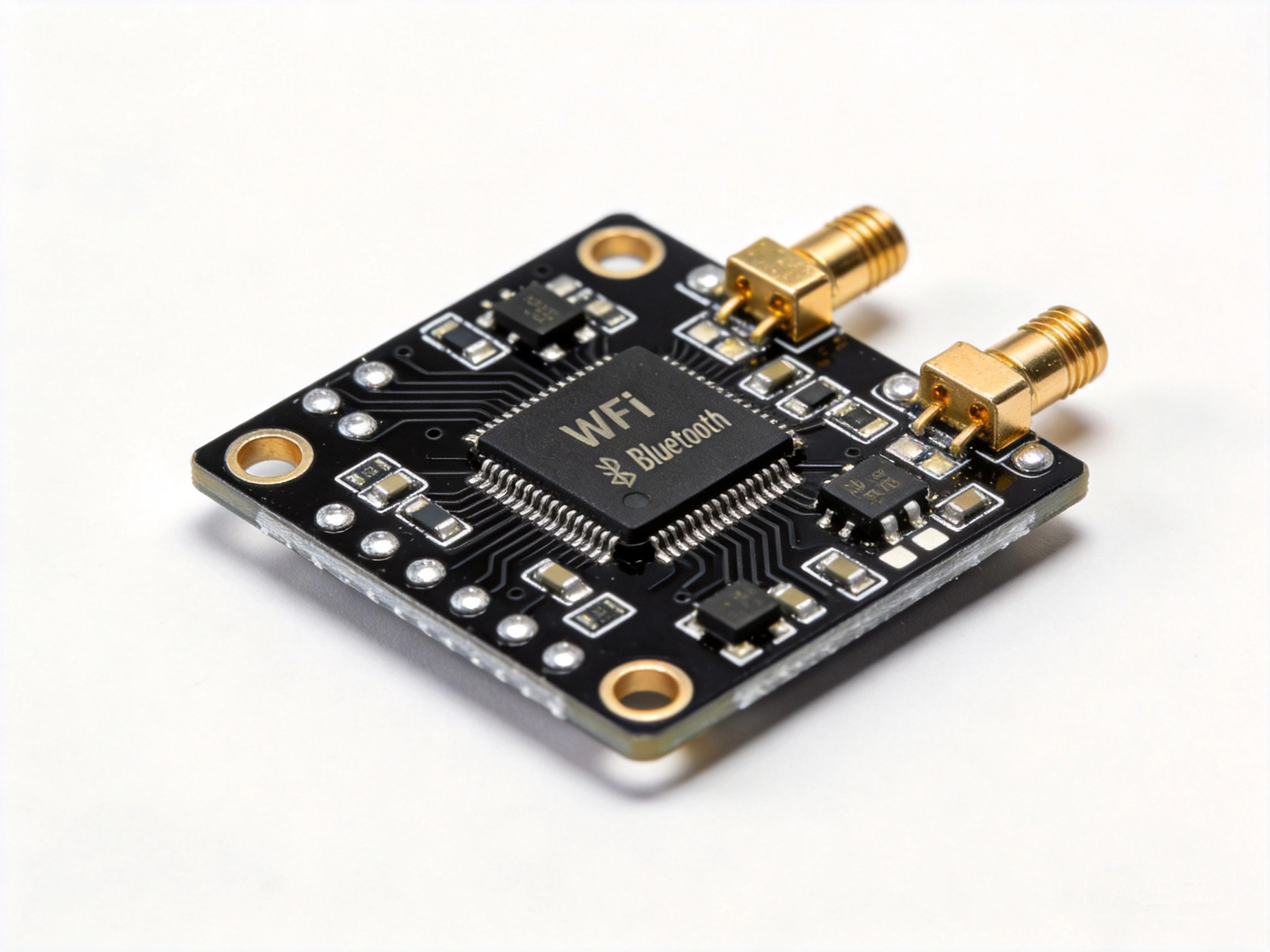
IoT and smart home devices operate across a range of frequency bands, each with its own regulatory constraints, propagation characteristics, and PCB design requirements. The most common bands are Wi-Fi at 2.4GHz and 5GHz, Bluetooth and Bluetooth Low Energy at 2.4GHz, Zigbee at 2.4GHz, and Thread at 2.4GHz. Emerging devices are beginning to use the 6GHz band (Wi-Fi 6E and Wi-Fi 7) and millimeter-wave frequencies for high-bandwidth applications such as high-resolution video streaming and low-latency gaming.
At 2.4GHz, the wavelength in free space is approximately 12.5 centimeters. On a PCB with a Dielectric Constant of 4.4 (standard Fr-4), the guided wavelength is approximately 6 centimeters. This means that a quarter-wave Transmission Line on a standard PCB is about 1.5 centimeters long. At these dimensions, the physical geometry of the PCB, the placement of components, and the routing of Transmission Lines all become significant factors in RF performance. A Transmission Line that is slightly too long or too short, or routed too close to a noisy digital circuit, can degrade the signal enough to reduce wireless range or increase packet error rate.
At 5GHz and 6GHz, the wavelength shrinks further, making the design sensitivity even greater. The quarter-wave length at 5GHz on Fr-4 is approximately 9 millimeters, which is comparable to the size of small passive components. At these frequencies, even the proximity of a Decoupling Capacitor to a wireless chip can affect impedance. This level of geometric sensitivity requires a more rigorous approach to Pcb Layout than most digital designers are accustomed to.
The choice of PCB laminate material has a direct and significant effect on RF performance. Standard FR-4, with its glass weave structure and moderate Dielectric Constant, is adequate for many low-frequency digital applications but introduces performance limitations at GHz frequencies. The dielectric constant of FR-4 varies with frequency, temperature, and resin content, creating impedance variability that is unacceptable for high-performance RF designs. The glass weave itself creates inhomogeneity in the dielectric, causing propagation delay variations that affect Signal Integrity at high frequencies.
For IoT devices that require reliable RF performance but must also meet aggressive cost targets, the most common solution is mid-range Pcb Materials that balance RF performance with cost. These include materials with tailored dielectric constants, tighter thickness tolerance, and more consistent glass weave styles than standard FR-4. Rogers Ro4003c and similar ceramic-hydrocarbon composites are popular for IoT applications where the performance gain over FR-4 justifies the higher material cost, while Isola I-Speed and Panasonic Megtron 6 offer improved performance at costs between FR-4 and high-end RF laminates.
The trend in IoT Pcb Materials is toward integration. More manufacturers are offering RF modules as pre-certified subsystems that integrate the antenna, matching network, and RF front-end on a small module that is designed to be mounted on the main PCB. These modules, based on chips with integrated radios, dramatically simplify the main PCB design by moving the most sensitive RF circuitry to a certified module with known performance characteristics. The main PCB must still be designed carefully, but the highest frequency signals are contained within the module.
The antenna is the most critical and the most challenging RF component in an IoT device. It must radiate efficiently across the device's operating frequency band, integrate physically with a compact enclosure, and coexist with other electronic components that may interfere with its radiation pattern. For smart home devices, where industrial design is as important as technical performance, the antenna often must be invisible to the consumer, embedded within the plastic enclosure or behind a decorative surface.
The most common antenna types in IoT devices are printed inverted-F antennas (PIFAs), planar inverted-F antennas (PIFAs), and chip antennas. PIFA antennas can be printed directly on the PCB and are cost-effective, but they require a clear Ground Plane beneath them and careful management of the near-field environment. Chip antennas are small ceramic components that are mounted on the PCB and offer a compact alternative to printed antennas, but they require careful matching network design and are sensitive to nearby conductors.
The proximity of the antenna to other components, particularly the battery and display, is one of the most common sources of RF performance degradation in IoT devices. Metals, including battery cases and display backplanes, absorb and reflect RF energy, reducing antenna efficiency and shifting the resonant frequency. Faraday cage effects from metallic enclosures require careful antenna placement or the use of antenna windows (areas of the enclosure without conductive material) to allow radiation to escape. PCB designers must work closely with mechanical engineers during the industrial design phase to ensure that the antenna has adequate clearance and that metallic components are positioned to minimize interference.
Compact IoT devices pack digital processors, wireless transceivers, power management circuits, sensors, and passive components into the smallest possible enclosure. This density creates an electromagnetic environment where RF signals, digital switching noise, and power supply ripple all coexist in close proximity. Managing the interactions between these signals is one of the most demanding aspects of IoT PCB design.
Power supply noise is a primary concern. The switching regulators that step down battery voltage to the rails needed by the wireless chip generate noise across a wide frequency range. If this noise couples into the RF front-end, it can desensitize the receiver or generate spurious emissions that violate regulatory limits. The solution involves careful power supply filtering, with ferrite beads and bypass capacitors placed as close as possible to the RF chip's power pins, and the use of separate power domains for the RF and digital sections.
Grounding strategy in high frequency IoT PCBs requires a different approach than conventional digital board Grounding. In digital boards, a continuous Ground Plane is preferred. In high frequency RF boards, the ground plane must be carefully managed to provide a consistent reference impedance for Transmission Lines while preventing ground loops and unwanted coupling. The ground return path for RF signals must be as short and direct as possible, and any gaps or slots in the ground plane beneath the RF transmission lines must be avoided because they cause impedance discontinuities and radiation.
The consumer demand for smaller and more discreet smart home devices is pushing PCB designers toward higher density solutions. HDI (High Density Interconnect) technology, with its microvia structures and fine-line capability, enables the routing density needed to place all required components on smaller boards, reducing the device footprint and enabling new product form factors. A smart speaker that once required a 100mm by 100mm board can now fit its electronics on a 40mm by 40mm board using HDI technology.
The most common HDI approach for IoT devices is a simple one-build or two-build HDI structure with microvias connecting the surface layer to the first inner layer. This level of HDI complexity adds modest cost to the board but enables significant area reduction by allowing Component Placement on both sides of the board with dense routing between layers. For the highest-density devices, any-layer HDI structures allow routing on all layers with microvia connections throughout, enabling the most compact board designs possible.
The challenge with HDI in IoT applications is the trade-off between miniaturization benefit and cost. HDI boards cost more per square centimeter than standard multilayer boards, and the cost difference becomes significant at high volumes where the per-unit premium is multiplied across millions of devices. The decision to use HDI must be justified by a clear product requirement for size reduction that cannot be achieved with standard board technology.
The transition from Wi-Fi 6 to Wi-Fi 6E and Wi-Fi 7 represents a significant step change in the RF performance requirements for smart home devices. Wi-Fi 6E introduces the 6GHz band, which offers wider channel bandwidths and lower latency than the crowded 2.4GHz and 5GHz bands. Wi-Fi 7 pushes data rates to 30Gbps and above using techniques such as 4096-QAM modulation and multi-link operation across multiple frequency bands simultaneously. Both of these developments place significantly higher demands on PCB materials, antenna design, and RF front-end performance.
The 6GHz band presents new PCB design challenges. At 7GHz, the quarter-wave length on standard PCB material is approximately 6 millimeters. The antenna, matching network, and transmission lines must all be designed with tolerances measured in fractions of a millimeter to achieve the required Impedance Matching and radiation efficiency. Standard Pcb Manufacturing tolerances, which are acceptable at 2.4GHz, become insufficient at 6GHz and above without special controls or RF-specific calibration.
The move toward integrated RF solutions is accelerating as a result. Radio chip manufacturers are integrating more RF functionality onto the wireless SoC, reducing the number of external components and the sensitivity of the RF performance to Pcb Layout variations. This integration trend simplifies the main PCB design but places greater responsibility on the chip manufacturer to ensure that the integrated radio meets performance requirements across all operating conditions.
The challenge for high frequency IoT PCBs is achieving the required RF performance at costs compatible with consumer electronics pricing. A smart thermostat may retail for USD 100, but the electronics inside it must be produced at a cost that supports that price point while delivering reliable wireless connectivity for years of operation. This requires a manufacturing approach that optimizes cost without sacrificing the RF performance that the product depends on.
One of the most effective cost optimization strategies is to minimize the RF-sensitive area of the PCB and use standard materials outside that area. The high frequency sections of the board, including the antenna, matching network, and critical transmission lines, can be fabricated on a small region of high-performance material, while the rest of the board uses standard FR-4. This hybrid construction reduces the area of expensive material while concentrating the Rf Design effort where it matters most.
Panel utilization during manufacturing is another cost lever. High frequency IoT PCBs are often small, with board areas of 25 square centimeters or less. Panelizing these boards efficiently requires placing multiple boards in a standard panel, which must be done carefully to avoid placing high-frequency components near the panel edges where the RF characteristics may differ from the board center. Designers should coordinate with the manufacturer on panel arrangement to optimize utilization without compromising RF performance.
Every IoT device that emits radio waves must be certified by the applicable regulatory authority before sale. In the United States, the FCC (Federal Communications Commission) certifies intentional radiators under FCC Part 15. In Europe, the Radio Equipment Directive (RED) sets the requirements. Similar regulations exist in every major market. These certifications require that the device meets defined limits for conducted and radiated emissions, and that the antenna and RF front-end perform within specified parameters.
The PCB design directly affects certification outcomes. A board with poor Impedance Control, inadequate grounding, or insufficient filtering may pass bench testing but fail radiated emissions testing in a certified test chamber. The cost of failing certification testing is significant: redesign, retesting, and schedule delay all add to the product cost. Investing in RF-aware PCB design from the first layout, rather than attempting to fix RF issues after certification testing, is the most cost-effective approach.
Pre-compliance testing, using bench-top equipment and basic antenna measurement setups, is increasingly common as a first step before formal certification testing. While pre-compliance testing does not replace certified testing, it can identify the most obvious RF issues early in the development cycle, reducing the risk of late-stage certification failures. Manufacturers with Rf Design expertise can provide pre-compliance evaluation as part of their design review service, helping to identify and resolve RF issues before the product reaches certification testing.
The IoT market is growing faster than any other segment of consumer electronics, driven by the continuing expansion of smart home ecosystems, industrial IoT applications, and wearable devices. Each new generation of IoT device demands higher data rates, lower latency, longer battery life, and smaller form factors, all of which translate into more demanding requirements for the PCB at the heart of each device.
The integration trend will continue. As wireless SoCs incorporate more RF functionality, the complexity of the main PCB design will decrease, but the importance of the PCB area dedicated to the antenna and RF front-end will increase. The antenna will remain the most challenging aspect of high frequency IoT PCB design, and the designers who master antenna integration in compact, consumer-friendly form factors will be in high demand.
New materials and manufacturing techniques will expand the designer's toolkit. Embedded antenna structures, where the antenna is built into the PCB rather than mounted on its surface, are under active development. These structures can reduce the sensitivity of antenna performance to enclosure effects and free up board space for other components. While still in relatively early stages, embedded antenna technology is expected to become more widely available as manufacturing processes mature.
high frequency pcb technology has become essential infrastructure for the IoT and smart home device industry. The frequency bands, material requirements, antenna integration challenges, and signal integrity considerations that were once the domain of specialized RF engineers are now mainstream knowledge for consumer electronics designers. The ability to design and manufacture high frequency PCBs cost-effectively at consumer electronics volumes has become a competitive differentiator for device makers, and the demand for skilled high frequency pcb designers will only grow as IoT devices become more capable and more pervasive.
The key to success in this space is understanding that High Frequency Pcb design for IoT is not a scaled-down version of aerospace RF design. It is a distinct discipline that balances RF performance against aggressive cost constraints, compact form factors, consumer industrial design requirements, and high-volume manufacturing processes. Designers who master this balance, working closely with manufacturers who understand the specific challenges of high frequency IoT PCBs, are well-positioned to capture the significant opportunity in this growing market.
Yes, FR-4 can be used for Wi-Fi PCBs at 2.4GHz for many consumer applications where moderate range and reliability are acceptable. However, FR-4's dielectric constant variation and glass weave effects can cause impedance variability that may reduce wireless range or increase error rates compared to higher-performance materials. For products where maximum range and reliability are important, mid-range materials such as Rogers Ro4003c or Isola I-Speed offer a better balance of RF performance and cost.
The most critical factor is managing the electromagnetic environment around the antenna. This means ensuring adequate clearance from conductive materials (batteries, displays, metallic enclosures), providing a consistent ground plane reference, and minimizing coupling between the antenna and noisy digital circuits. Industrial design constraints often conflict with ideal antenna placement, making early collaboration between electrical and mechanical engineers essential.
HDI technology enables higher routing density on smaller boards, allowing more functionality to be placed on compact PCBs that fit inside smaller enclosures. This is particularly valuable for smart home devices where form factor is a key competitive factor. HDI also enables Component Placement on both sides of the board and supports microvia structures that reduce the routing area required for interconnections.
Wireless IoT devices require radio certification from the applicable regulatory authority in each market where they are sold. In the United States, this means FCC certification. In Europe, it means CE marking under the Radio Equipment Directive. Each certification requires testing of radiated emissions, conducted emissions, and RF performance parameters. The PCB design must support compliance with these requirements.
Wi-Fi 6E and Wi-Fi 7 operate at higher frequencies and use wider modulation bandwidths than previous Wi-Fi generations, placing greater demands on PCB materials, Impedance Control, and antenna design. The 6GHz band used by Wi-Fi 6E requires tighter manufacturing tolerances and more precise antenna matching than the 2.4GHz band. Wi-Fi 7's multi-link operation adds further complexity by requiring the PCB to support simultaneous operation across multiple frequency bands.
Top High Frequency PCB Applications in the 5G and Telecommunications IndustryMay/29/2026
Handling Sensitive ComponentsMay/29/2026
A Deep Dive into High Frequency PCB Capabilities for Millimeter Wave TechSeptember/24/2026
The Ultimate Guide to High Frequency PCB Materials: PTFE, Ceramic, and HydrocarbonJuly/08/2026
Understanding Thermal Stability in High Frequency PCB MaterialsAugust/10/2026
High Frequency PCB Assembly for Automotive Radar: Precision and ReliabilitySeptember/21/2026
From Prototype to Mass Production: Scaling with a Reliable High Frequency PCB ManufacturerJuly/13/2026

Essential High Frequency PCB Knowledge for Hardware Engineers and DesignersJune/15/2026