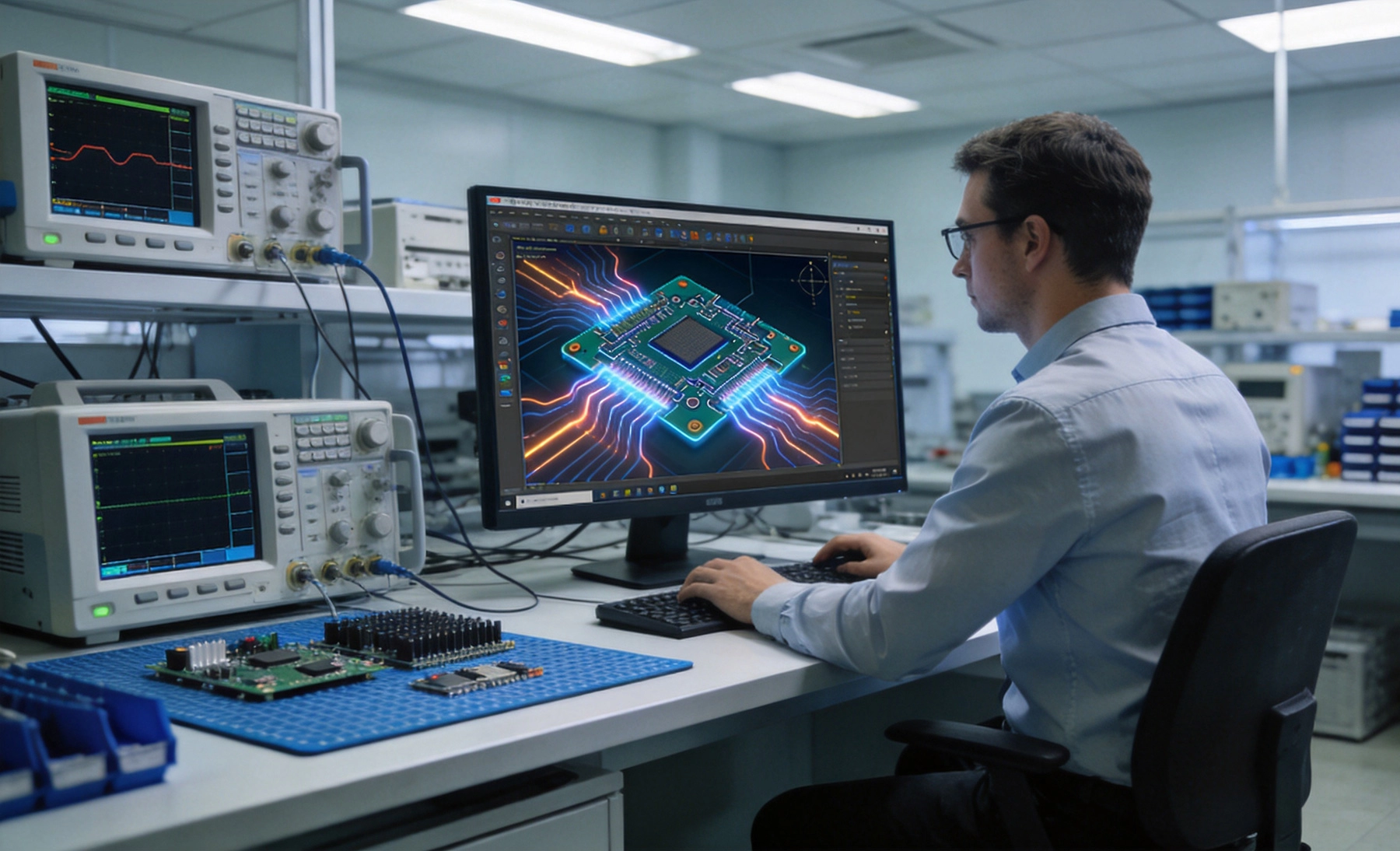
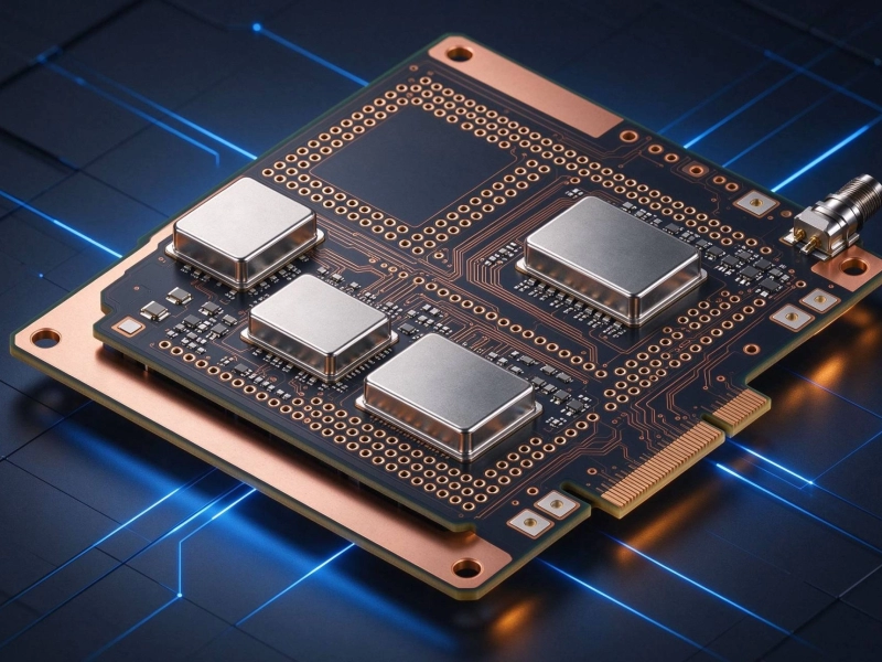
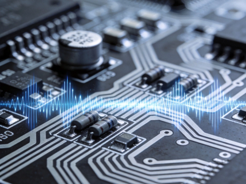
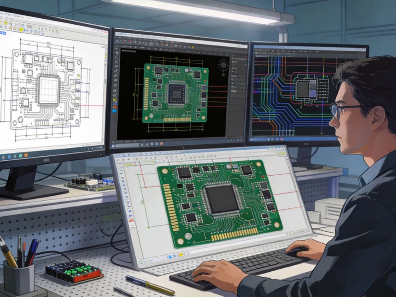
High frequency PCBs operating at 1GHz and above (including 5G millimeter-wave systems, radar applications, high-speed digital links, and RF communications equipment) present unique design challenges that cannot be addressed through traditional design methodologies. At these frequencies, electromagnetic effects that are negligible at lower frequencies become dominant, often leading to unexpected performance issues, signal degradation, and compliance failures. Electromagnetic simulation tools have become indispensable for modern high frequency PCB design, allowing engineers to predict performance, optimize designs, and reduce costly physical iterations before manufacturing.

Core Challenges of High Frequency PCB Design
As signal frequencies increase, several electromagnetic phenomena become critical design considerations that can make or break product performance:
-
Impedance Mismatch: Even minor variations in trace impedance can cause significant Signal Reflection, leading to reduced power transfer, signal distortion, and increased bit error rates in digital systems.
-
Signal Integrity Issues: High-speed signals suffer from attenuation, dispersion, and timing jitter that can corrupt data and prevent reliable communication, especially in multi-gigabit serial links.
-
Electromagnetic Compatibility (Emc/Emi): High frequency circuits are prone to unintended electromagnetic radiation that can cause interference with other systems and fail regulatory compliance testing.
-
Crosstalk: Electromagnetic coupling between adjacent traces can cause signal interference, leading to false triggering and reduced noise margins.
-
Parasitic Effects: Previously negligible features such as via holes, component pads, and trace corners introduce significant parasitic inductance and capacitance at high frequencies, disrupting circuit performance.
-
Increased Power Loss: High frequency operation leads to higher conductor losses (Skin Effect) and dielectric losses, reducing efficiency and causing Thermal Management challenges.
Traditional trial-and-error design approaches, where multiple prototype iterations are manufactured and tested, become prohibitively expensive and time-consuming for high frequency designs. Each design iteration typically costs thousands of dollars and takes weeks to complete, delaying product launch and increasing development costs. Simulation tools eliminate much of this guesswork by allowing virtual testing and optimization before physical manufacturing.
Key Simulation Technologies for High Frequency PCBs
Modern high frequency design relies on several complementary simulation technologies to address different aspects of performance:
1. Electromagnetic (EM) Simulation
Em Simulation is the foundation of high frequency PCB design, calculating how electromagnetic fields interact with PCB structures:
-
2D/2.5D Em Simulation: Fast, cost-effective simulation for planar structures such as Transmission Lines, power planes, and simple RF components. Ideal for impedance calculation, crosstalk analysis, and planar filter design.
-
3D EM Simulation: Accurate full-wave simulation of complex 3D structures including via transitions, antenna systems, BGA packages, and complex RF components. Provides comprehensive analysis of radiation, coupling, and parasitic effects that 2D simulators miss.
Leading EM simulation tools include ANSYS HFSS, CST Studio Suite, and Keysight ADS, which offer different solver technologies optimized for specific use cases.
2. Signal Integrity (SI) Simulation
Signal Integrity simulation focuses on the quality of signal transmission through the PCB:
-
Predicts Signal Reflection, attenuation, crosstalk, and timing jitter
-
Generates eye diagrams to visualize signal quality and bit error rate (BER) performance
-
Validates compliance with high-speed interface standards (PCIe 5.0/6.0, DDR5, 100G Ethernet, etc.)
-
Optimizes equalization and pre-emphasis settings for long-reach links
3. Power Integrity (PI) Simulation
Power integrity simulation analyzes the power distribution network (PDN) to ensure stable Power Delivery to high frequency components:
-
Calculates PDN impedance across the operating frequency range to ensure it meets target impedance requirements
-
Predicts voltage ripple and noise caused by fast switching currents
-
Optimizes Decoupling Capacitor selection and placement to minimize noise
-
Identifies potential ground bounce and power supply noise issues
4. Thermal Simulation
High frequency circuits often dissipate significant power, making thermal simulation critical:
-
Predicts temperature distribution across the PCB under operating conditions
-
Identifies hot spots that could reduce component reliability or cause performance drift
-
Optimizes heat sink design, copper placement, and thermal via placement
-
Validates that component temperatures stay within specified operating ranges
5. Multi-Physics Co-Simulation
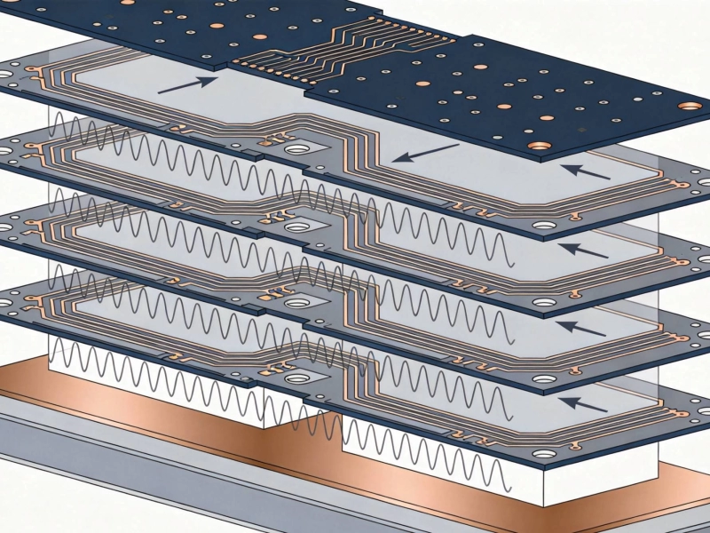
Advanced design flows combine EM, SI, PI, and thermal simulation to analyze how different physical phenomena interact:
-
Temperature changes affect material properties and component performance, which in turn affect EM performance
-
Power dissipation from Rf Circuits affects thermal performance
-
Mechanical stress from vibration or thermal expansion can affect high frequency performance, especially in millimeter-wave applications
Integrating Simulation into the High Frequency Design Workflow
To achieve maximum benefit, simulation should be integrated at every stage of the high frequency pcb design process:
Concept and Stackup Design Stage
-
Simulate different material options (high-frequency laminates from Rogers, Taconic, Isola, etc.) to select the optimal Dielectric Constant (Dk) and loss tangent (Df) for your application
-
Model different stackup configurations to achieve target impedance requirements for critical signals
-
Simulate Transmission Line geometries (Microstrip, stripline, coplanar waveguide) to determine optimal trace widths and spacing
-
Validate power plane architecture to meet power integrity requirements early in the design process
Component Placement and Routing Stage
-
Simulate critical Component Placement to minimize coupling between sensitive Rf Circuits and noisy digital circuits
-
Model via transitions to optimize their impedance performance and minimize signal reflection at high frequencies
-
Simulate trace routing options to minimize crosstalk and Signal Loss in critical paths
-
Optimize matching network component values for RF circuits before Component Placement
Pre-Manufacturing Verification Stage
-
Run full-board signal integrity simulation to validate all high-speed links meet performance requirements
-
Perform Emi simulation to predict radiated emissions and ensure compliance with regulatory standards (FCC, CE, etc.)
-
Simulate complete power distribution network performance across the entire operating frequency range
-
Validate antenna performance (gain, efficiency, radiation pattern) for wireless devices
Prototype Validation Stage
-
Compare simulation results with measured performance from Prototype Testing to validate and calibrate simulation models
-
Use simulation to identify the root cause of any unexpected measured performance issues
-
Update simulation models with measured material and component parameters for improved accuracy in future designs
Common Simulation Use Cases for High Frequency Designs
Simulation tools solve a wide range of common high frequency design challenges:
-
Impedance Matching Optimization: Simulate and optimize matching networks for RF components, antennas, and high-speed links to maximize power transfer and minimize return loss.
-
Via Design Optimization: Optimize via anti-pad dimensions, stub lengths, and Grounding strategies to minimize impedance discontinuities at high frequencies.
-
Emi Reduction: Simulate different Shielding strategies, filtering approaches, and layout modifications to reduce radiated emissions and ensure compliance with regulatory requirements.
-
High-Speed Link Validation: Simulate end-to-end performance of multi-gigabit serial links to ensure eye diagrams remain open across all operating conditions.
-
Antenna Integration: Simulate on-board antenna performance in the presence of other components and enclosures to optimize placement and achieve required radiation characteristics.
-
Filter Design: Design and optimize RF filters directly in simulation to achieve required passband, stopband, and Insertion Loss characteristics before manufacturing.
Best Practices for Effective High Frequency Simulation
To get the most accurate and useful results from high frequency simulation:
-
Use Accurate Material Parameters: Obtain frequency-dependent Dk and Df values from material manufacturers, as these properties change significantly with frequency. Using incorrect material data is the most common cause of simulation-to-measurement discrepancies.
-
Appropriately Mesh Simulation Models: Balance simulation accuracy and speed by using finer meshes only in critical areas with high field gradients, while using coarser meshes in less critical regions.
-
Include All Relevant Structures: Don't simplify models excessively. Include component pads, solder masks, and mounting structures that can affect high frequency performance.
-
Calibrate Models with Measured Data: Regularly compare simulation results with measured data from prototypes to refine your simulation models and improve accuracy over time.
-
Focus on Critical Paths: Don't waste time simulating every part of the board. Focus simulation efforts on high-risk, high-frequency paths that are most likely to have performance issues.
-
Validate Simulation Setup: Always verify simulation results with simple test structures first to ensure your setup and boundary conditions are correct before simulating complex designs.
Business Benefits of Simulation-Driven High Frequency Design
Investing in simulation capabilities delivers significant return on investment for high frequency product development:
-
Faster Time to Market: Reduce design iterations from an average of 3-5 to 1-2, cutting development time by months and enabling earlier product launch.
-
Lower Development Costs: Eliminate the cost of multiple prototype iterations, each costing thousands of dollars in manufacturing and testing expenses.
-
Higher Performance Products: Simulation enables design optimization that is not possible through trial and error, resulting in better signal integrity, lower power consumption, and higher reliability.
-
Reduced Compliance Risk: Identify and resolve EMI issues early in the design process, ensuring first-time pass of regulatory compliance testing and avoiding costly redesigns.
-
Improved Product Reliability: Simulation helps identify potential failure modes before manufacturing, resulting in more robust products with lower field failure rates.
Future Trends in High Frequency PCB Simulation
Simulation technology continues to evolve to meet the demands of increasingly complex high frequency designs:
-
AI-Driven Design Optimization: Machine learning algorithms are being integrated with simulation tools to automatically optimize design parameters and find optimal solutions much faster than manual methods.
-
Cloud-Native Simulation: Cloud-based simulation platforms allow access to virtually unlimited computing resources, enabling faster simulation of large, complex designs without requiring expensive local hardware.
-
Shift-Left Simulation: Simulation is being integrated earlier into the design flow, even at the schematic capture stage, to identify issues before significant design investment is made.
-
Integrated Design-Simulation Workflows: Tighter integration between ECAD design tools and simulation platforms is reducing the time and effort required to set up simulations, making simulation accessible to more design engineers.
Conclusion
Electromagnetic simulation tools have become essential for successful high frequency pcb design, enabling engineers to address the complex challenges of operating at GHz and millimeter-wave frequencies. By integrating simulation at every stage of the design process, companies can reduce development time, lower costs, improve product performance, and ensure reliable operation of high frequency circuits. As high frequency applications continue to expand with 5G, 6G, Automotive Radar, and high-speed digital systems, simulation will become even more critical to maintaining competitive advantage in the electronics industry.
Contact us to discuss your requirements.