At radio frequencies (RF) and microwave frequencies, grounding and shielding cease to be simple "connect to ground" tasks and become critical Signal Integrity Challenges. A poor ground plane or inadequate shielding can introduce parasitic inductance, create ground loops, radiate EMI, and degrade the performance of even the most carefully designed high-frequency circuit. This article covers the fundamental principles, best practices, and common pitfalls of grounding and shielding in high-frequency PCB design.

1. Why Grounding and Shielding Matter at High Frequencies
At low frequencies (DC to a few MHz), a ground connection behaves like a low-impedance node. But as frequency increases, several phenomena change the game:
- Parasitic inductance dominates: Every trace and via has inductance (~1 nH/mm for a typical trace). At 1 GHz, a 5 mm trace has an inductive reactance of approximately 31 Ω—far from a "short to ground."
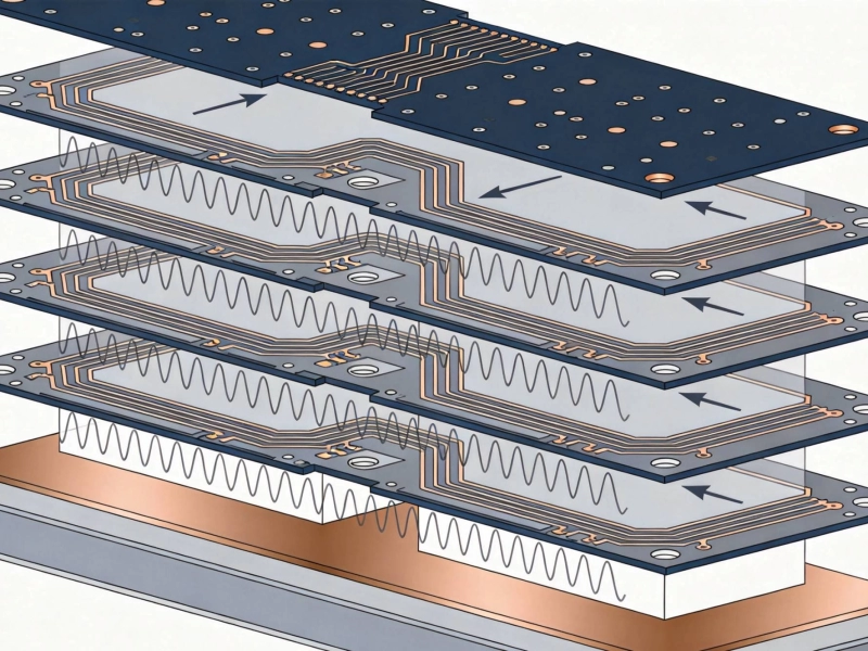
- Return current follows the path of least inductance: At high frequencies, return currents flow directly beneath the signal trace on the adjacent reference plane (ground or power). Any discontinuity in this plane forces the return current to take a longer path, increasing loop area and radiating EMI.
- Ground becomes a distributed network: The ground plane is no longer an equipotential surface. Voltage differences can exist across the plane due to finite conductivity and inductance.
- Cavity resonances: Large, un-stitched ground/power plane pairs form parallel-plate waveguides that can resonate at specific frequencies, creating standing waves and radiating strongly.
These effects mean that grounding and shielding must be designed as integral parts of the high-frequency signal path, not as afterthoughts.
2. Grounding Fundamentals for High-Frequency PCBs
2.1 The Ground Plane: Your Most Important Shield
A solid, continuous ground plane directly beneath signal traces is the single most effective grounding technique for high-frequency designs. Key principles:
- Use a dedicated ground layer: In multilayer boards, allocate at least one full layer as an unbroken ground plane. Avoid splitting the ground plane unless absolutely necessary.
- Keep signal traces close to their reference plane: The closer the signal trace is to the ground plane, the smaller the current loop area and the lower the radiation. For microstrip lines, typical dielectric thickness is 0.1–0.2 mm for RF layers.
- Avoid slots and cuts in the ground plane: Any gap in the ground plane beneath a high-frequency trace forces the return current to detour, increasing loop inductance and creating an antenna. If a split is unavoidable, bridge it with multiple stitching capacitors or 0-Ω resistors.
- Use thin dielectric between signal and ground: Thinner prepreg reduces the Characteristic Impedance variation and improves return path continuity. For 50 Ω microstrip on Fr-4, a 0.1 mm dielectric requires a trace width of ~0.18 mm; on Rogers Ro4003c (Dk ≈ 3.38), it requires ~0.22 mm.
2.2 Via Stitching and Ground Vias
Vias connect ground planes across layers and provide low-inductance return paths. Best practices:
- Stitch ground planes frequently: Place ground vias at intervals of ≤ λ/20 (where λ is the shortest wavelength of interest) along ground plane boundaries and around high-frequency traces. As a rule of thumb, use via spacing of 3–5 mm for designs up to 6 GHz, and ≤ 2 mm for designs above 10 GHz.
- Place ground vias near signal vias: When a signal trace changes layers, place one or more ground vias within 0.5–1 mm of the signal via to provide a continuous return path. This is called a "via return stub" or "ground via companion."
- Use multiple vias in parallel: Two vias in parallel halve the inductance. For critical RF connections (e.g., SMA connector ground pins, filter grounds), use 3–4 vias in a via fence pattern.
- Avoid via stubs: In thick boards, the unused portion of a via (the "stub") acts as a resonant antenna. Use back-drilling to remove via stubs for frequencies above ~5 GHz, or use blind/buried vias.
2.3 Grounding Strategies: Single-Point vs. Multi-Point
| Strategy | Description | Best For | Caveats |
|---|
| Single-point (star) ground | All grounds connect to one physical point | Low-frequency analog, mixed-signal DC grounding | Long ground traces add inductance; not suitable for RF |
| Multi-point ground | Grounds connect to a low-impedance plane at many points | High-frequency / RF / microwave | Requires solid ground plane; watch for ground loops at lower frequencies |
| Hybrid (split plane with bridges) | Analog and digital grounds split but bridged at one point or with capacitors | Mixed-signal boards with both RF and digital | Bridging must be carefully designed; capacitors provide AC ground while maintaining DC isolation |
For high-frequency designs, multi-point grounding to a solid plane is almost always the correct choice. Star grounding introduces too much inductance above a few MHz.
2.4 Decoupling and Bypass Capacitors as AC Ground
Decoupling capacitors provide a local AC ground for IC power pins, shunting high-frequency noise to ground. Key considerations:
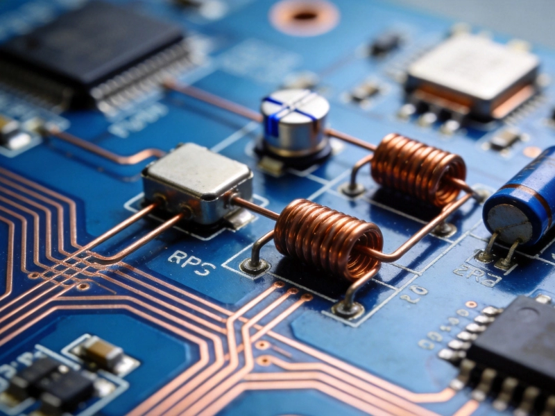
- Use multiple capacitor values: A typical decoupling network uses 100 nF (low-frequency bypass), 10 nF (mid-frequency), and 1 nF or 100 pF (high-frequency). Each capacitor has a self-resonant frequency (SRF); above the SRF, it becomes inductive.
- Place capacitors as close to the IC pin as possible: Every millimeter of trace adds inductance. Ideally, the capacitor pad should be directly adjacent to the IC pad.
- Use low-inductance capacitor packages: 0201 or 01005 packages have lower ESL than 0805. Reverse-geometry capacitors (e.g., 0508, 0306) have even lower inductance due to wider terminations.
- Use ground vias on both sides of the capacitor: This minimizes the loop area from IC pin → capacitor → ground plane.
3. Shielding Techniques for High-Frequency PCBs
3.1 Ground Pour and Copper Flood
Unused areas of signal layers should be flooded with copper connected to ground via numerous vias. This creates a Faraday cage effect and reduces radiation. Guidelines:
- Maintain clearance from signal traces: Keep a gap of at least 2× the trace-to-plane distance between the ground pour and high-frequency traces to avoid impedance discontinuities. For a 50 Ω microstrip with 0.15 mm dielectric, use ≥ 0.3 mm clearance.
- Stitch ground pours to the main ground plane: Use vias spaced ≤ 3 mm apart to connect the pour to the underlying ground plane. Ungrounded copper pours can become resonant antennas.
- Avoid isolated copper islands: Any copper not connected to ground can float and radiate. Ensure all copper pours have a DC path to ground.
3.2 Ground Walls and Via Fences
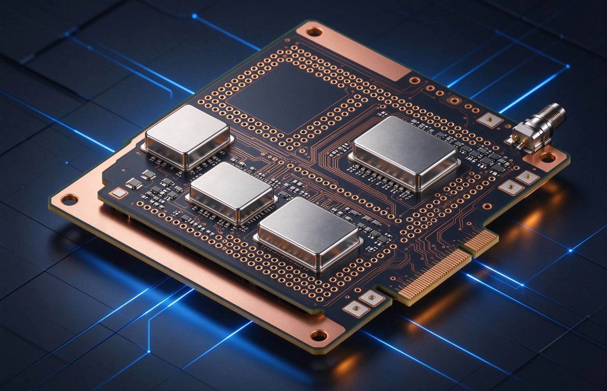
A via fence (also called a "picket fence" or "via wall") is a row of closely spaced ground vias that acts as a shield wall between circuits. Applications:
- Isolating RF sections: Place via fences between transmitter and receiver chains, or between different frequency bands, to reduce crosstalk.
- Shielding Transmission Lines: Grounded coplanar waveguide (GCPW) uses ground pours on either side of the signal trace, connected to the bottom ground plane with via fences. This provides better shielding than microstrip and is preferred for frequencies above 10 GHz.
- Board edge shielding: Place a via fence along the board edge (spacing ≤ λ/10 at the highest frequency of concern) to prevent edge radiation and reduce coupling to external structures.
Via fence design rule: Via spacing should be ≤ λg/10, where λg is the guided wavelength in the dielectric. For Fr-4 at 10 GHz, λg ≈ 15 mm, so via spacing should be ≤ 1.5 mm. For Rogers Ro4003c at 24 GHz, λg ≈ 7 mm, so spacing should be ≤ 0.7 mm.
3.3 Shielding Cans (Metal Enclosures)
For sensitive Rf Circuits (LNAs, VCOs, PLLs, power amplifiers), a metal shielding can soldered to the PCB provides the highest level of isolation. Design considerations:
- Ground the shield can frequently: The PCB should have a continuous ground ring under the shield can perimeter, with ground vias spaced ≤ 2 mm apart connecting to internal ground planes.
- Provide keep-out zones: Maintain ≥ 0.5 mm clearance between components and the shield can wall to avoid shorting and to allow for solder fillets.
- Consider Thermal Management: Shield cans trap heat. For power amplifiers, include thermal vias under the device to conduct heat to internal or bottom ground planes, or use shield cans with ventilation slots (keeping slot dimensions < λ/20 to maintain shielding effectiveness).
- Use conductive gaskets for removable shields: If the shield must be removable (for testing or repair), use EMI gaskets (conductive elastomer, wire mesh, or finger stock) to maintain RF continuity.
3.4 Cable and Connector Shielding
High-frequency signals entering or leaving the PCB via cables are major EMI pathways. Best practices:
- Use shielded connectors: SMA, SMB, MCX, and U.FL connectors have metal shells that should be soldered to the PCB ground plane with multiple ground vias.
- Ground the cable shield at the entry point: For coaxial cables, the shield should be grounded immediately where it enters the PCB enclosure. Avoid "pigtail" ground connections, which add inductance.
- Use feedthrough capacitors or filtered connectors: For DC power lines entering a shielded enclosure, use feedthrough capacitors or pi-filter connectors to prevent RF from leaking along the power line.
- Differential signaling for off-board links: LVDS, CML, or other differential interfaces are more resistant to common-mode noise than single-ended signals.
4. Common Grounding and Shielding Mistakes
4.1 Splitting the Ground Plane Under High-Speed Traces
This is the single most common mistake in high-frequency design. A split ground plane forces return currents to flow around the gap, creating a large loop antenna. Solution: Keep the ground plane solid under all high-frequency traces. If analog/digital separation is needed, route traces so they do not cross the split, or bridge the split with a carefully placed capacitor.
4.2 Long Ground Leads on Components
Using long wires or traces to connect a component's ground pin to the ground plane adds inductance. At 1 GHz, a 5 mm ground lead has ~30 Ω of reactance. Solution: Use surface-mount components with ground pads directly on the top layer, connected to the ground plane with short, wide vias (or thermal relief pads for solderability).
4.3 Insufficient Via Stitching
Ground planes on different layers that are not adequately stitched together can develop voltage differences and act as slot antennas. Solution: Place ground vias at every ground pad, at regular intervals along ground pours, and around the board perimeter.
4.4 Ignoring the Return Path
Designers often focus on the signal trace but neglect the return current path. Solution: Always ask, "Where does the return current flow?" For every signal trace, there should be an adjacent reference plane (ground or power) with no gaps. Use simulation tools to visualize return current density.
4.5 Mixing Analog and Digital Grounds Incorrectly
Connecting analog and digital grounds at multiple points creates ground loops that pick up digital noise. Connecting them at a single point with long traces creates high inductance for the analog ground. Solution: Use a solid ground plane, partition the board into analog and digital regions (not split planes), and route signals so that return currents do not cross region boundaries. Bridge the regions with a single 0-Ω resistor or ferrite bead if DC isolation is needed.
5. Simulation and Verification
Grounding and shielding designs should be verified with Electromagnetic Simulation before fabrication:
- 2.5D planar EM simulators (e.g., Keysight ADS Momentum, AWR AXIEM): Fast analysis of multilayer PCB structures, ground plane discontinuities, and via effects. Suitable for frequencies up to ~20 GHz.
- 3D full-wave EM simulators (e.g., Ansys HFSS, CST Microwave Studio): Accurate modeling of shielding cans, connector transitions, via fences, and cavity resonances. Essential for designs above 10 GHz or with complex 3D structures.
- Return current visualization: Most EM tools can plot current density on ground planes, revealing return path discontinuities before fabrication.
- Impedance and S-parameter extraction: Verify that grounding features (via fences, ground pours) do not introduce unexpected impedance discontinuities or resonances.
6. Material and Stackup Considerations
The choice of PCB material and stackup directly impacts grounding and shielding effectiveness:
- Low-loss Laminates: Rogers RO4000 series, Isola I-tera, and Panasonic Megtron 6 have lower dissipation factors than FR-4, reducing ground plane losses at microwave frequencies.
- Thin dielectrics: Thinner prepreg between signal and ground layers reduces loop inductance and improves shielding. For RF layers, use 0.1–0.2 mm dielectric thickness.
- Ground plane proximity: Place high-frequency signal layers adjacent to ground planes (e.g., Layer 1 signal, Layer 2 ground). Avoid routing RF traces on layers far from a ground reference.
- Controlled Impedance stackup: Work with your Pcb Manufacturer to design a stackup that achieves target impedances (50 Ω single-ended, 100 Ω differential) while maintaining solid ground references.
7. Quick Reference Checklist
| Checklist Item | Yes/No |
|---|
| Is there a solid, unbroken ground plane beneath all high-frequency traces? | |
| Are ground vias placed within 0.5–1 mm of every signal via transition? | |
| Are ground pours stitched to the main ground plane with vias ≤ 3 mm apart? | |
| Are via fences used to isolate sensitive RF sections (spacing ≤ λg/10)? | |
| Are decoupling capacitors placed as close to IC pins as possible, with ground vias on both sides? | |
| Are connector shells grounded with multiple vias (≥ 4 for SMA)? | |
| Are there any ground plane splits under high-speed traces? (If yes, fix before proceeding.) | |
| Has the design been verified with EM simulation for return current continuity? | |
| Are shield cans (if used) grounded with a continuous ring and vias ≤ 2 mm apart? | |
| Are cable shields grounded at the entry point without pigtails? | |
Conclusion
Grounding and shielding in high-frequency PCB design are not optional—they are fundamental to achieving acceptable Signal Integrity, EMI compliance, and circuit performance. The key principles are simple but require disciplined execution:
- Provide a solid, continuous ground plane as the primary return path for all high-frequency signals.
- Minimize loop areas by keeping signal traces close to their reference planes and using ground vias liberally.
- Stitch ground planes frequently with vias to prevent cavity resonances and maintain equipotential conditions.
- Use via fences and ground pours to isolate sensitive circuits and reduce crosstalk.
- Shield critical sections with metal cans when board-level techniques are insufficient.
- Verify with EM simulation before fabrication to catch return path discontinuities early.
By treating grounding and shielding as first-class design concerns from the start of the layout process, you can avoid the costly respins and compliance failures that plague many high-frequency PCB projects.