Open Nav

High-frequency printed circuit boards are no longer confined to laboratory instruments or telecom base stations. Today, they operate inside jet engines, deep-sea sensor arrays, satellite payloads, Automotive Radar modules, and industrial microwave systems. In these applications, electrical performance cannot be separated from environmental survival. A board that performs perfectly at room temperature may fail when exposed to thermal cycling, humidity, vibration, or sustained high power. This is why high frequency PCB Applications: Designing for Extreme Environments has become one of the most demanding topics in advanced electronics manufacturing.
Designing for extreme environments requires more than selecting a low-loss material. It demands a holistic approach that balances dielectric stability, Impedance Control, thermal management, mechanical reliability, and manufacturability. In this article, I will examine the key challenges engineers face when deploying high-frequency PCBs in harsh conditions, and how material selection, stack-up design, and process control determine long-term performance.
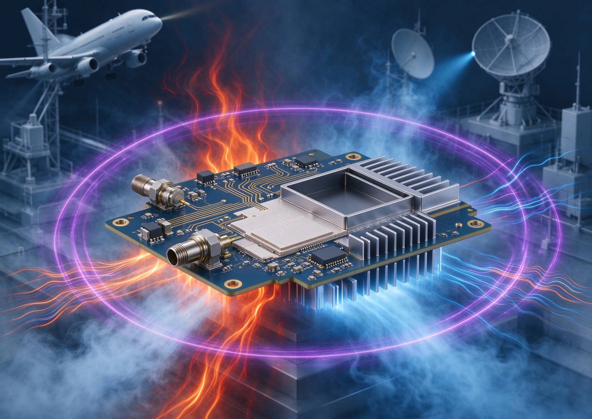
The term "Extreme Environment" covers a wide range of operating conditions. In high-frequency applications, the most critical stressors include:
Each of these factors can alter Dielectric Constant, increase Insertion Loss, shift resonant frequency, or create intermittent failures that are difficult to reproduce during standard testing.
Material choice is the single most important decision in High-frequency Pcb design. Unlike standard Fr-4 boards, high-frequency laminates must maintain stable electrical properties across temperature, frequency, and humidity variations.
Ptfe materials offer extremely low dielectric loss and stable performance at millimeter-wave frequencies. They are widely used in radar antennas, Satellite Communications, and high-speed test fixtures. However, Ptfe has a high coefficient of thermal expansion and can be difficult to process. In extreme thermal environments, PTFE boards often require specialized fillers, reinforced structures, or hybrid stack-ups to maintain mechanical reliability.
Ceramic-filled materials provide a useful compromise between RF performance and manufacturability. They typically offer better dimensional stability than pure PTFE and can be processed with more conventional PCB equipment. These laminates are common in Automotive Radar, 5G infrastructure, and industrial sensing applications where both electrical performance and environmental durability are required.
Polyimide and high-Tg laminates are often chosen for their thermal endurance and mechanical toughness. While they may not match the lowest-loss PTFE materials, they perform well in environments where thermal cycling, flexing, or high-temperature operation is the dominant concern. They are frequently used in aerospace, defense, and rigid-flex high-frequency assemblies.
A well-designed stack-up does more than route signals. In extreme environments, it must maintain consistent impedance, minimize thermal stress, and protect sensitive RF structures.
High-frequency Transmission Lines are highly sensitive to dielectric thickness variation. In harsh environments, moisture absorption or thermal expansion can change effective Dielectric Constant and shift impedance. Selecting materials with low moisture absorption and tight thickness tolerance helps maintain performance over the product lifetime.
Interrupted ground planes create return-path discontinuities that become more severe at higher frequencies. In vibration-prone environments, poor ground continuity can also increase the risk of intermittent connections. Continuous reference planes, closely spaced ground vias, and careful via placement help preserve Signal Integrity and mechanical robustness.
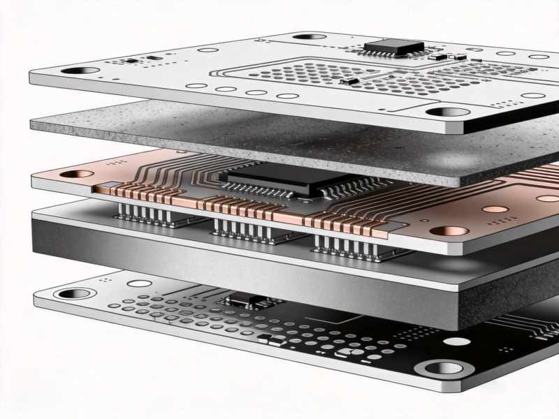
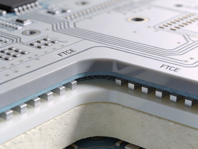
Many extreme-environment systems use hybrid stack-ups that combine low-loss RF layers with mechanically robust digital or power layers. This approach allows designers to optimize each section of the board for its specific function. For example, a radar module may use a low-loss substrate for antenna layers while relying on a tougher material for control circuitry and connectors.
High-frequency circuits often generate significant heat, especially in power amplifiers, transmit modules, and high-speed processors. In extreme environments, this heat cannot simply dissipate into ambient air. Elevated ambient temperatures reduce thermal headroom and accelerate material aging.
Effective thermal management begins with layout. High-power components should be placed near thermal vias, metal cores, or heat sinks. Copper thickness, via density, and thermal pad design all influence junction temperature. In sealed enclosures, internal temperature rise can be much higher than external readings suggest, so thermal simulation should reflect worst-case operating conditions rather than idealized laboratory environments.
Moisture is one of the most underestimated threats to high-frequency PCBs. Water absorption increases dielectric loss, shifts impedance, and can cause delamination during thermal cycling. In outdoor or marine applications, salt fog and corrosion further threaten exposed copper and solder joints.
Surface finish selection plays an important role here. ENIG provides good planarity and corrosion resistance, making it suitable for fine-pitch components and moderate RF applications. ENEPIG offers additional reliability for wire bonding and harsh environments. For high-frequency antenna surfaces, bare copper with protective coatings may be used, but coating thickness and dielectric properties must be carefully modeled to avoid performance drift.
Automotive radar, avionics, and industrial sensors must survive continuous vibration and mechanical shock. High-frequency boards are often more vulnerable because their performance depends on precise geometry. A micro-crack in a Transmission Line, a failing via barrel, or a lifted pad can degrade RF performance long before a complete electrical failure occurs.
Design practices that improve mechanical reliability include using filled vias, avoiding acute trace angles, reinforcing heavy component areas, and ensuring adequate annular rings. In rigid-flex designs, bend radius control and strain relief become critical. For through-hole connectors carrying RF signals, mechanical retention and solder joint integrity must be validated under vibration profiles that match the intended application.
Simulation alone cannot guarantee reliability. High-frequency PCBs destined for extreme environments should undergo environmental stress screening that reflects real-world use. Common qualification methods include thermal cycling, humidity testing, salt fog testing, vibration testing, and high-temperature storage. RF performance should be measured before and after environmental exposure, because some failures appear only as gradual changes in Insertion Loss, return loss, or phase stability.
Early collaboration with the Pcb Manufacturer is essential. Processes such as Controlled Impedance testing, microsection analysis, moisture bake-out, and plasma desmear can significantly affect final reliability. Design rules that work for consumer electronics may not be sufficient for aerospace, automotive, or industrial deployments.
High-frequency Pcb design for extreme environments is a multidisciplinary challenge. It requires stable materials, disciplined stack-up planning, careful thermal management, and robust mechanical construction. The best designs do not simply achieve target RF performance on paper; they maintain that performance after repeated thermal cycles, prolonged humidity exposure, and sustained vibration. As radar, satellite, automotive, and industrial systems continue to push into higher frequencies and harsher operating conditions, mastering high frequency PCB Applications: Designing for Extreme Environments will remain essential for engineers who need both precision and durability.
There is no single best material. PTFE-based laminates offer excellent RF performance, ceramic-filled materials provide better mechanical stability, and polyimide or high-Tg materials excel in high-temperature applications. The optimal choice depends on frequency, power level, environmental stress, and manufacturing capability.
Moisture increases dielectric loss, shifts impedance, and can cause delamination during thermal cycling. Materials with low moisture absorption and appropriate surface protection are essential for outdoor, marine, and aerospace applications.
Standard Fr-4 may be acceptable for lower microwave frequencies or non-critical control circuits, but it is generally unsuitable for high-performance RF, millimeter-wave, or extreme-environment applications due to higher loss and less stable dielectric properties.
Handling Sensitive ComponentsMay/29/2026
High Frequency PCB Applications: Designing for Extreme EnvironmentsOctober/13/2026
How to Source Reliable Industrial SMT PCB Assembly from Trusted China ManufacturersJuly/29/2026
High Frequency PCB Prototype vs. Mass Production: Key Differences in FabricationJune/05/2026
From Design to Reality: A Step-by-Step Guide to Ordering a High Frequency PCB PrototypeSeptember/20/2026
Hybrid Stack-ups: Combining FR4 and RF Materials in High Frequency PCB FabricationSeptember/14/2026
How to Choose the Best High Frequency PCB Prototype Supplier for StartupsSeptember/10/2026
The Ultimate Guide to High Frequency PCB Materials: PTFE, Ceramic, and HydrocarbonJuly/08/2026