Open Nav

High frequency printed circuit boards are no longer confined to controlled laboratory environments or sheltered communication rooms. Today, they operate in Automotive Radar modules exposed to road salt and thermal cycling, in 5G outdoor base stations facing humidity and UV radiation, in aerospace systems enduring vacuum and extreme temperature swings, and in industrial sensors subjected to vibration and chemical contamination. Designing high frequency PCBs for these extreme environments requires more than selecting a low-loss material. It demands a coordinated approach across material science, stackup design, manufacturing process control, environmental protection, and reliability verification.
This article explains how extreme environments affect high frequency PCB performance, which materials and structures are most suitable, and what design practices help maintain Signal Integrity and long-term reliability.
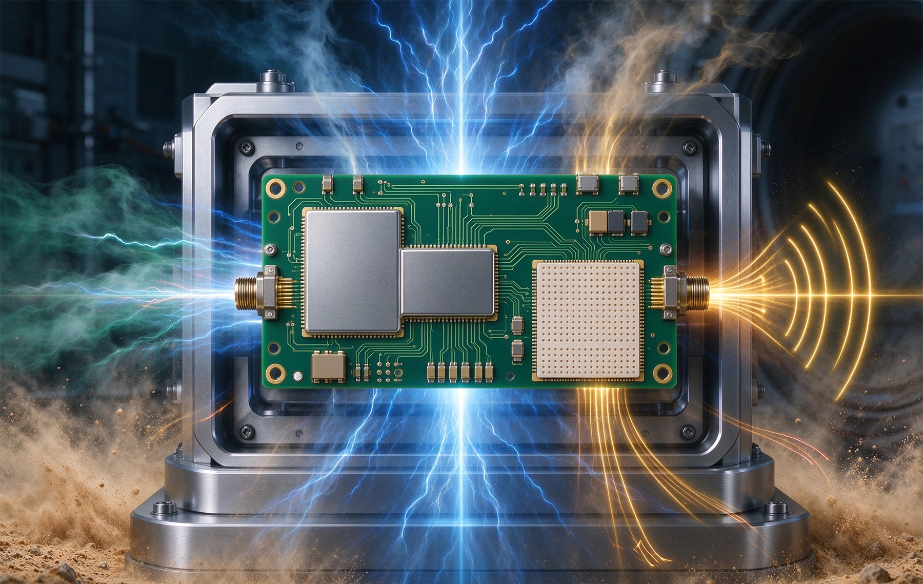
An extreme environment is any condition that pushes a PCB beyond normal commercial operating ranges. For high frequency applications, the most common stressors include:
These factors do not only affect mechanical reliability. They can directly degrade high frequency performance by changing impedance, increasing Insertion Loss, shifting resonant frequency, and reducing phase consistency across antenna arrays.
Water has a much higher Dielectric Constant than most PCB resins. When a laminate absorbs moisture, its effective Dielectric Constant, or Dk, can shift, causing impedance deviation and Signal Reflection. In high frequency circuits, even small Dk changes can detune antennas, shift filter response, and degrade phase alignment. Materials with low moisture absorption, such as PTFE-based laminates and certain ceramic-filled hydrocarbon systems, are therefore preferred for humid or outdoor applications.
High frequency PCBs often use thin Transmission Lines, controlled-impedance structures, and dense via fields. During thermal cycling, differences in the coefficient of thermal expansion, or CTE, between copper, resin, and glass fiber create mechanical stress. Over time, this stress can cause via barrel cracking, pad separation, or interlayer delamination. For aerospace and automotive applications, where temperature swings may be repeated thousands of times, via reliability becomes a primary design constraint.
Vibration does not only threaten large connectors. It also affects RF components, Shielding cans, antennas, and high-frequency modules mounted on thin substrates. Without proper mechanical support, solder joints can develop fatigue cracks, leading to intermittent RF performance or complete Signal Loss. This risk increases when heavy components are placed far from mounting points or when the PCB itself is too thin for the expected vibration profile.
High frequency circuits are sensitive to surface conditions because much of the current flows near the conductor surface at high frequencies. Corrosion on copper traces, pads, or connector interfaces increases resistance and can disturb impedance continuity. In salt fog or sulfur-rich industrial environments, unprotected copper and certain surface finishes may degrade quickly.
Material selection is the first line of defense. For high frequency PCBs in extreme environments, engineers must balance electrical performance, thermal stability, mechanical strength, manufacturability, and cost.
PTFE, or polytetrafluoroethylene, materials offer extremely low dielectric loss and excellent high frequency stability. They are widely used in Satellite Communications, millimeter-wave radar, phased-array antennas, and high-performance RF systems. PTFE laminates also have very low moisture absorption, which helps maintain stable Dk and Df in humid conditions. However, PTFE materials can be difficult to process. They often require special drilling, surface activation, and lamination procedures, and their CTE may differ significantly from copper.
Ceramic-filled hydrocarbon laminates, such as Rogers Ro4350b and related families, provide a practical middle ground. They offer stable Dk, low Df, better dimensional stability than pure PTFE, and processing compatibility closer to conventional multilayer PCBs. These materials are commonly used in 5G infrastructure, Automotive Radar, industrial RF modules, and mixed-signal boards where both high frequency performance and manufacturability matter.
Standard Fr-4 is generally unsuitable for critical high frequency signal layers above a few gigahertz because its loss increases significantly with frequency and its Dk varies with moisture and temperature. However, high-Tg Fr-4 can still play a useful role in hybrid stackups. In such designs, high frequency signal layers use Low-loss Materials, while power, ground, or low-speed control layers use more cost-effective FR-4. This approach reduces cost while protecting the most sensitive RF paths.
Copper roughness affects conductor loss at high frequencies. Smooth or very low profile copper helps reduce Insertion Loss, especially above 10 GHz. Surface finish selection also matters. Electroless nickel immersion gold, or ENIG, is frequently used because it provides a flat surface, good solderability, and reasonable corrosion resistance. For harsh environments, conformal coating, thick solder mask, or additional protective layers may be required to prevent moisture ingress and chemical attack.
Impedance Control is central to high frequency PCB design. In extreme environments, impedance stability depends on more than trace width and dielectric thickness. It also depends on how consistently the material maintains its Dk across temperature, humidity, and frequency.
Designers should consider the following:
In phased-array antennas and millimeter-wave systems, phase consistency across channels is often as important as insertion loss. Material CTE, lamination uniformity, and copper thickness variation can all affect electrical length, so stackup symmetry and process control become critical.
High frequency circuits do not only suffer from external heat. They also generate heat through dielectric loss, conductor loss, and active RF components such as power amplifiers. In extreme environments, elevated ambient temperature reduces thermal headroom and accelerates aging.
Effective thermal strategies include:
For automotive and aerospace applications, thermal design must also consider long-term reliability. Repeated thermal cycling can weaken via barrels and solder joints even when steady-state temperatures remain within specification.
Moisture protection is especially important for outdoor and industrial high frequency PCBs. Water absorption can change dielectric properties, while salts and industrial pollutants can corrode copper and degrade connectors.
Common protection methods include:
One caution is that conformal coating itself can affect high frequency performance. If the coating has a different dielectric constant than air, it may shift impedance or resonant frequency. Therefore, RF-critical areas should be simulated with the coating included, or protected by Shielding rather than direct coating.
High frequency PCBs in vehicles, aircraft, and industrial equipment must survive sustained vibration and occasional shock events. Mechanical design is not separate from Rf Design because component movement, board flexing, and connector fatigue can all degrade Signal Integrity.
Recommended practices include:
For aerospace radar and satellite systems, rigid-flex PCBs can reduce the number of connectors and cables, thereby improving both mechanical reliability and high frequency performance. Fewer interconnects mean fewer impedance discontinuities and fewer potential failure points under vibration.
Automotive radar modules, especially those operating at 77 GHz, must maintain stable antenna performance across wide temperature ranges, humidity, vibration, and exposure to road chemicals. Material Dk stability, low moisture absorption, and precise Impedance Control are essential. Hybrid stackups combining high frequency laminates with FR-4 structural layers are common in these designs.
Outdoor 5G antennas and remote radio units face solar heating, rain, humidity, and thermal cycling. Their antenna arrays require consistent phase response across many channels. Moisture-induced Dk shift or uneven thermal expansion can distort beamforming performance. Low-loss, low-absorption materials and robust environmental sealing are therefore critical.
Aerospace high frequency PCBs must survive extreme temperatures, vacuum, radiation, and launch vibration. Materials must have low outgassing, stable electrical properties, and reliable interlayer bonding. PTFE-based and ceramic-filled laminates are often used, sometimes in rigid-flex configurations to eliminate fragile connectors.
Industrial sensors used in chemical plants, power systems, and manufacturing lines may encounter corrosive gases, oil mist, vibration, and wide temperature swings. High frequency PCBs in these systems benefit from conformal coating, corrosion-resistant finishes, thick copper for mechanical strength, and careful isolation between RF and power circuits.
Designing for extreme environments is incomplete without verification. High frequency PCBs should be tested not only for electrical performance but also for environmental durability.
Typical tests include:
The most valuable insight comes from comparing RF performance before and after environmental stress. A PCB may pass visual inspection yet still show increased insertion loss, shifted resonance, or degraded return loss after thermal cycling or humidity exposure.
high frequency pcb applications in extreme environments require a systems-level approach. Low-loss Materials are necessary but not sufficient. Designers must also control impedance stability, manage thermal stress, protect against moisture and corrosion, reinforce mechanical structures, and validate performance after environmental exposure. The most reliable designs are those that treat electrical performance and environmental durability as inseparable requirements.
As high frequency systems move further into automotive, aerospace, industrial, and outdoor infrastructure markets, the ability to maintain signal integrity under harsh conditions will become a defining competitive advantage. Success depends on choosing the right materials, designing for real-world stress, and verifying performance through rigorous environmental testing.
FR-4 has relatively high dielectric loss, unstable Dk at high frequencies, and higher moisture absorption than dedicated high frequency laminates. These characteristics can cause excessive insertion loss, impedance drift, and performance variation under temperature and humidity stress.
PTFE-based laminates, ceramic-filled hydrocarbon materials, and hybrid stackups combining high frequency layers with FR-4 are commonly used. The choice depends on frequency, loss budget, environmental exposure, and manufacturability.
Yes. Conformal coating changes the dielectric environment around RF traces and can shift impedance or resonant frequency. Critical RF areas should be simulated with the coating included, shielded, or selectively masked.
Use adequate board thickness, mounting points, stiffeners, and mechanically robust connectors. Avoid unnecessary RF layer transitions, and consider rigid-flex designs to reduce connector count in high-vibration systems.
Thermal cycling, humidity testing, salt fog testing, vibration testing, and post-stress RF measurements are among the most important. Electrical performance should be verified after environmental exposure, not only before it.
How to Source Reliable Industrial SMT PCB Assembly from Trusted China ManufacturersJuly/29/2026
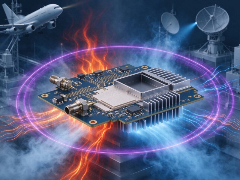
High Frequency PCB Applications: Designing for Extreme EnvironmentsOctober/15/2026
Handling Sensitive ComponentsMay/29/2026
Common Pitfalls to Avoid During Your High Frequency PCB Prototype PhaseJune/18/2026
Inside the Factory: What to Look for in a High Frequency PCB Manufacturer's FacilityAugust/03/2026
Turnkey High Frequency PCB Prototype Services: Streamlining Your Development CycleAugust/06/2026
Advanced High Frequency PCB Knowledge: Using Simulation Tools for Better ResultsSeptember/29/2026
How to Test and Verify the Quality of High Frequency PCB MaterialsOctober/14/2026